With the rise of chip interconnection, the circuit structure has become more complex, and the threat of hidden defects to the good rate has increased significantly. How to detect short circuits, broken circuits and other problems and accurately dispose of them without destroying the circuit is the first task in the field of semiconductor integrated circuits to improve device performance and good efficiency.
Driven by this demand, laser technology has entered the public eye with its characteristics, opening new paths for circuit detection and repair.
When conducting electrical testing, it is often necessary to remove the insulating layer on the device surface or the electrodes of voltage-sensitive devices, thereby enabling inspection of the underlying electrodes and circuit structures。At this stage, the mainstream approaches still rely on mechanical window opening, chemical etching two traditional methods, which have long faced the following pain points:
Against this background, realizing the full-process closed loop of “lossless peeling insulation layer – accurate detection – high success rate repair” has promoted the deep application of laser technology in the field of precision circuit detection and repair.
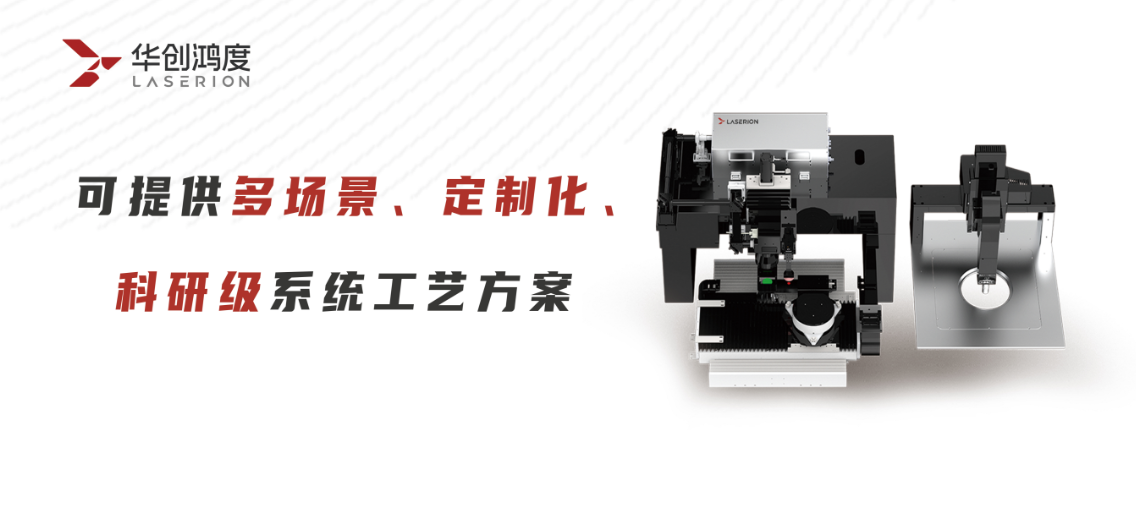
Huachuang Hongdu relies on core light source advantages to customize targeted process solutions, forming a complete closed-loop system of “oxide layer removal, detection, and repair.”
① Laser stripping – high accuracy and lossless opening of windows
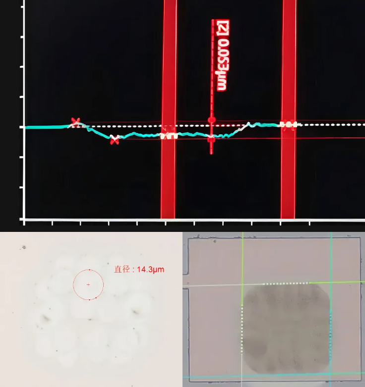
△ Microscopic Measurement of Electrode Oxidation Layer Removal by Femtosecond Laser Processing
The goal of the stripping process is to precisely remove the insulating layer or oxide layer without damaging the underlying circuitry, thereby exposing the test electrodes or traces. A femtosecond laser“Precise energy regulation, combining processing quality and efficiency, No thermal accumulation effect. The performance advantages enable the removal of oxide layers with an area precision of ≤1 μm² and a residual oxide volume of ≤1%, without damaging the electrodes. After completing the stripping, confirm the normal function of the electrodes through electrical re-inspection, precisely locate the fault points, and then proceed with the subsequent steps. Precise laser repair of circuit defects.
② Laser Repair – High Precision Repair of Circuit Defects
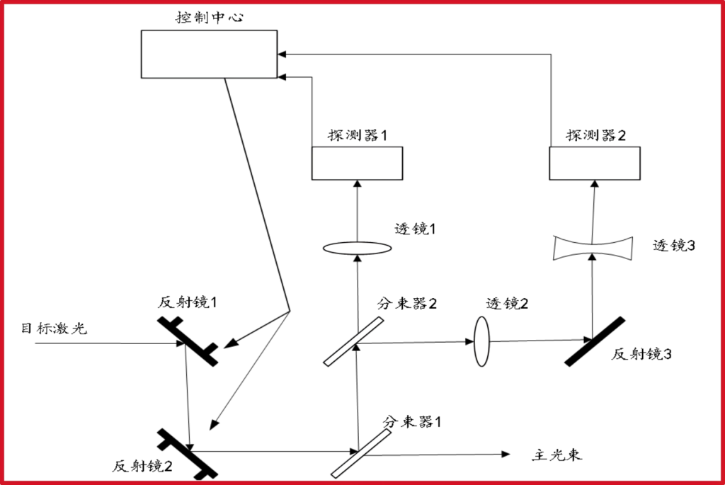
△ High-stability Precision Optical System
An open circuit refers to a break (such as scratches, corrosion, or material defects) in an otherwise continuous circuit, resulting in signal interruption。 Using laser-induced localized deposition thin film technology, it can accurately “bridge” the fault and restore the electrical connection. The principle is to use high-energy ultraviolet pulse lasers to bombard the target so that it vaporizes instantly and forms a plasma glow.Under the heating induced by infrared laser, the material in Yuhui deposits and epitaxially grows into a film at substrate defect sites, thereby achieving film repair area precision ≤1 μm² with high precision and controllable repair.
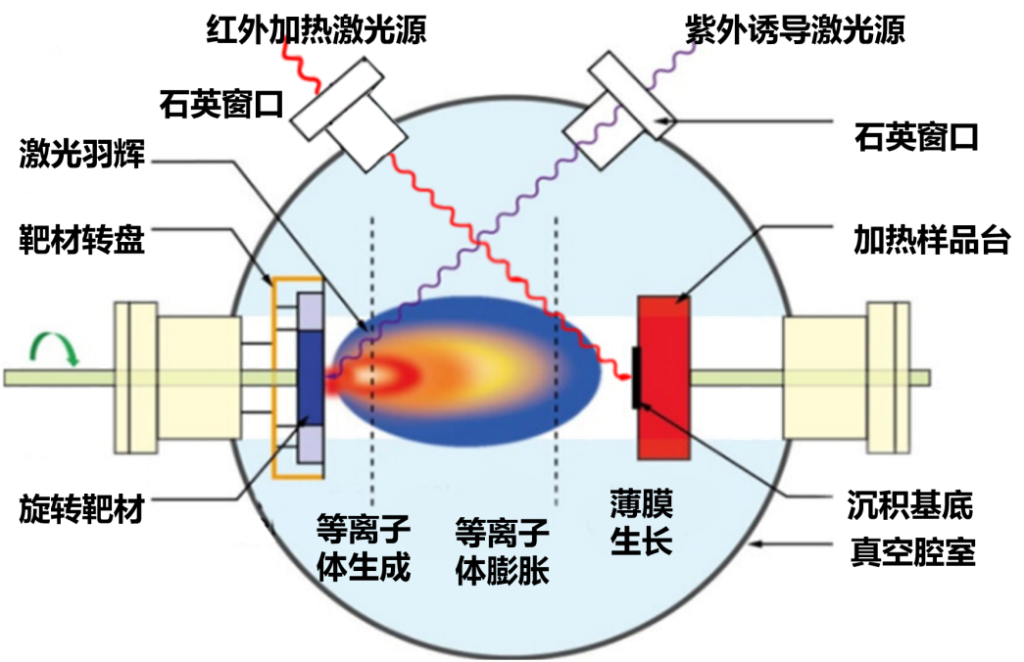
△ Laser-assisted Vapor Deposition Process: Multi-physics Field Coupling – Technical Principles
Short circuits are typically caused by metal residue, bridging, or dielectric breakdown, manifesting as abnormal conduction between adjacent lines. Femtosecond laser processing leverages its characteristics of “high precision” and “cold processing” to vaporize and remove excess metal or conductive residues without damaging surrounding circuits。 By actively controlling the light source direction and matching the focal length of the variable-focus objective lens, it is possible to achieve a short-circuit defect repair area accuracy of ≤ ±1 μm². n addition, compared to in-situ grown thin film technologies without lithography, laser repair offers greater flexibility and repair efficiency.
③ Laser fire reduction – high-precision localized heat induced modification
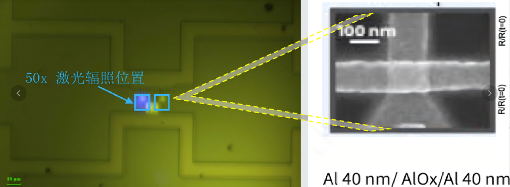
△ Microstructure of Annealed Test Samples is S hown
Laser annealing employs localized precision heat treatment to reduce surface defects and impurities on the circuit, improve local structure and electrical performance, and precisely correct abnormal resistance values. By precisely regulating specific wavelength laser parameters, the target area is heated to the desired temperature range in a very short time and then cooled quickly.Combining high-stability lasers with dual-color radiation temperature measurement technology, it ensures annealing temperature stability of ≤±1°C, annealing repair positioning accuracy of ≤±1μm, ultimately achieving a single induction accuracy of ±5Ω and increasing the resistance value of the repaired area by 10~50%.
The above three key processes and inspection steps are deeply integrated, forming a closed-loop process of “stripping-inspection-repair-re-inspection,” while also supporting fully automated loading and unloading modules, significantly improving yield and efficiency.
The reason this laser processing technology scheme can be stably implemented lies fundamentally in the autonomous control over the core light source—this is precisely the capability foundation of Huachuang Hongdu. We focus on high-reliability solid-state laser technology , and have currently established a complete technical pathway ranging from core light source research and mass production to testing of laser application processes in new scenarios and with new materials。 Welcome enterprises and research institutions to engage in in-depth discussions and obtain customized support, jointly contributing to the steady development of China’s intelligent manufacturing and its “chips.”