
On back-contact (BC) production lines, “use the shortest wavelength available” is still a common first instinct. It sounds conservative. It is not always correct for rear dielectric grooving—especially when the station must open AlOx/SiNx-class stacks cleanly and still hit industrial wafers-per-hour without doubling scanner count.
“On a back-contact (BC) rear grooving qualification, the first instinct was ‘use UV picosecond—safer for everything.’ Coupon work on AlOx/SiNx-class dielectric opens looked clean at low speed, but the line model could not hold target wafers-per-hour without stacking more scanners than the tool budget allowed. We re-ran the same open window with a 532 nm green picosecond source in the ≥120 W industrial band, ~10 ps pulses, fluence held near the selective-open threshold so the silicon substrate stayed intact. Green absorption on the dielectric stack gave a usable process window; average power and 400–2000 kHz-class repetition headroom recovered throughput. UV stayed on the shortlist for a-Si:H-sensitive HJT-like stacks, but for this BC dielectric grooving station it was over-spec. The decision was not ‘green is better lasers’—it was ‘green matches this open, at a power the line can afford.’” — PV process engineer, BC rear dielectric grooving line qualification
That scene is why the title question matters for process engineers and equipment integrators alike. Choosing a green picosecond laser for BC solar cell grooving is not a branding preference. It is a station-level trade among film absorption, passivation budget, and commercially defensible line speed.
Use a green picosecond laser for BC solar cell grooving when the job is selective open of dielectric or passivation stacks—typically AlOx/SiNx-class membranes—with minimal damage to the underlying crystalline silicon, and when industrial average power is required to hold wafers-per-hour. Around 532 nm and ~10 ps, green picosecond sources often sit between infrared, which can couple too deeply into the wafer, and ultraviolet, which can be excellent for ultra-fragile films but easier to over-specify on capital cost and throughput. Hold fluence near the ablation threshold of the film you intend to remove. Nameplate peak power is not the acceptance metric.
BC architectures place both polarities on the rear and remove front-grid shading. The efficiency story is compelling; the manufacturing story is stricter. Rear surfaces must carry interdigitated contact geometries, dielectric opens, and metallization interfaces that do not erase the passivation advantage that justified moving to BC in the first place. As PERC approached practical ceilings and the industry shifted toward TOPCon, heterojunction (HJT), and BC families, laser stations stopped being laboratory curiosities. They became the maskless path that makes high-efficiency rear structures printable at gigawatt scale.
Across that history, laser roles multiplied: selective emitters, rear dielectric ablation for PERC-class contacts, poly-finger localization, back-contact isolation, and laser-assisted metallization. Not every one of those jobs wants the same pulse family. Nanosecond pulses support “hot” work—melt-assisted doping, sintering, and contact engineering—where thermal diffusion is useful or at least tolerable. Picosecond and femtosecond pulses support “cold” opens, where energy must leave before heat wrecks thin dielectrics, a-Si:H stacks, or carefully tuned poly-Si/SiOx contacts. BC grooving, in the sense most production RFQs mean it, usually lives on the cold side of that fork: you are clearing films to create a metallization-ready geometry, not intentionally forming a deep melt pool.
Wavelength sits inside that cold choice. Optical absorption depth, thin-film interference, and the exact layer stack decide whether 1064 nm, 532 nm, or 355 nm opens a workable window between incomplete dielectric removal and substrate damage. Green is not universally superior. It is frequently the practical band when the grooving station must combine selective membrane open with industrial average power and stable groove geometry across a full wafer.
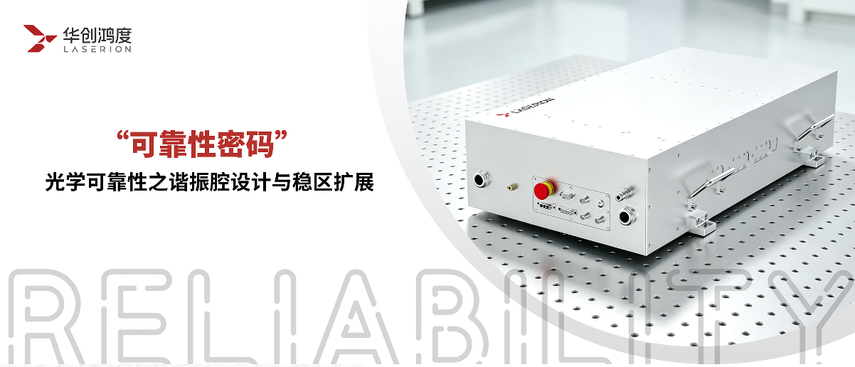
Laserion’s position in that discussion is deliberate. We supply industrial ultrafast laser sources for mid-market production cells, including PV process stations. We do not sell a competing turnkey BC tool. Integrators own scanners, wafer handling, metrology, and cell process IP. Our job is to make the green picosecond band checkable on an RFQ: 532 nm, ≥120 W, ~10 ps, pulse energy >300 µJ, M² <1.3, RMS ≤0.8%, with programmable Burst Mode when the qualified recipe needs temporal splitting.
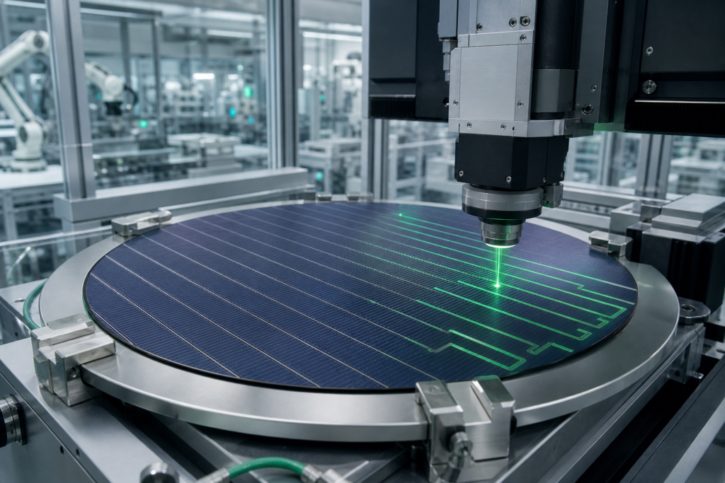
BC rear grooving is frequently a film problem before it is a silicon problem. The laser must clear a dielectric or passivation membrane—AlOx, SiNx, or related stacks—without treating the wafer bulk as the primary absorber. Infrared picosecond sources carry high pulse energy and are excellent on many brittle-material and wafer-scribing sister tools, but at 1064 nm the optical interaction can push deeper into the stack. That narrows the window between “dielectric gone” and “silicon melted or defected,” especially when operators raise energy to chase throughput.
Ultraviolet picosecond light couples strongly and can be the right answer for ultra-thin, temperature-fragile layers. HJT-like a-Si:H patterning is the classic example. The mistake is assuming every BC grooving station is that example. Many BC and PERC-adjacent rear opens are dielectric membrane grooving jobs where green around 532 nm improves coupling into the films that must leave, while keeping the interaction more surface-weighted than infrared.
That absorption match is why green picosecond sources appear in backside membrane grooving and TCO-adjacent patterning discussions: selective removal with a process window wide enough for production scanners. It is also why fluence discipline matters. Even a well-chosen green beam will damage silicon if the operator runs far above film threshold “to be safe.”
How to judge on the line: Write the exact film stack and thicknesses into the RFQ. Run open-threshold or single-shot crater curves at candidate wavelengths on the real stack, not on a generic coupon. Accept green when the dielectric clears at a fluence that leaves silicon free of melt features in SEM and without catastrophic lifetime collapse in photoluminescence maps. If the critical layer is dominated by ultra-thin a-Si:H, keep ultraviolet on the shortlist and do not force green for political consistency.
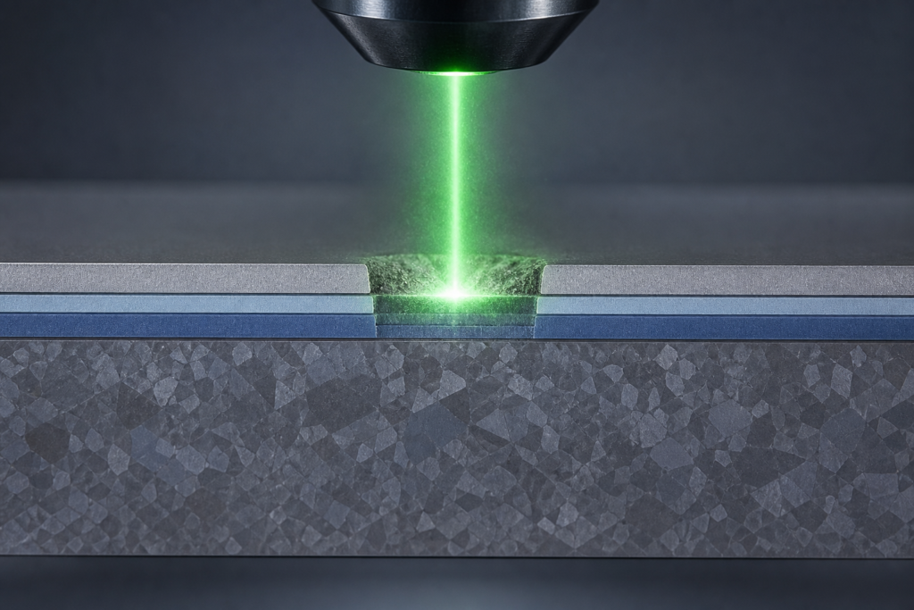
BC efficiency is passivation-sensitive by design. Laser edges that look acceptable under a microscope can still inject recombination that shows up later as open-circuit voltage loss, fill-factor scatter, or dark regions on PL. Nanosecond dielectric opens often look inexpensive on the laser purchase order and expensive after wet recovery, scrap, and missed efficiency bins. The pulse is long enough for significant thermal diffusion relative to thin-film thicknesses, which is exactly the wrong habit when the rear stack is the performance product.
Picosecond pulses—around 10 ps in industrial green platforms—deposit energy on a timescale that supports cold film removal when fluence stays near threshold. For grooving, the practical signatures are sharp dielectric edges, less recast, fewer melt features in the silicon, and a narrower heat-affected zone (HAZ) than nanosecond opens at comparable removal rates. Green wavelength and picosecond duration work as a pair: wavelength selects where energy couples; pulse width limits how far heat travels while the film is leaving.
Integrators should translate that physics into FAT language. Do not approve a grooving source on average watts alone. Require before-and-after lifetime or PL on opened wafers, groove-width capability across the wafer, and a written fluence window with upper and lower bounds. Industrial green picosecond bands that publish RMS ≤0.8% and M² <1.3 are publishing the stability class that keeps groove geometry from walking as the scanner writes thousands of features. Pulse-to-pulse wander near threshold is not a cosmetic issue; it is incomplete opens in one region and substrate damage in another.
If your next BC coupon matrix is already booked, freeze wavelength and fluence against the dielectric stack drawing before you freeze scanner count. Changing from an ultraviolet tooling assumption to a green optical train mid-build usually means a second mechanical and controls loop, not a software toggle.
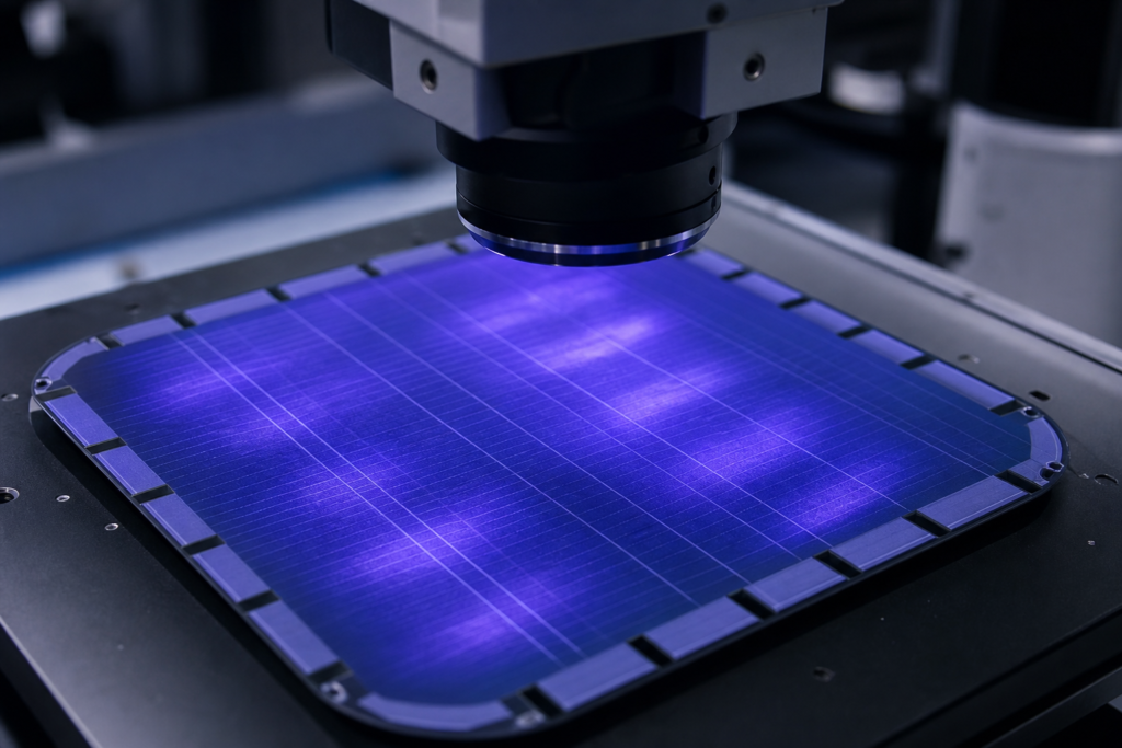
Coupon quality and factory quality are different optimization problems. Ultraviolet picosecond can win a carefully staged laboratory open and still lose the line model when average power forces more scanners, more floorspace, or slower wafers-per-hour to hold the same edge quality. BC factories do not ship champion coupons; they ship distribution. That is where green picosecond platforms in the ≥120 W class, with 400–2000 kHz-class repetition headroom and >300 µJ-class pulse energy, earn their place.
Throughput math should be done at the fluence that meets passivation criteria, not at the maximum nameplate power. A source that can only make the open beautiful at half the required UPH is not a production grooving laser yet. Likewise, Burst Mode should enter the RFQ only when the qualified recipe uses subpulse packets for cleaner or faster dielectric removal. Programmable burst—pulses per burst, interval, and energy distribution—is then a first-class configuration item. If the process never leaves single-pulse or simple pulse-repetition-frequency operation, unused burst scope becomes change-order risk without process benefit.
Beam delivery details matter at production power. Pointing stability and spot uniformity support DOE or multi-lane shaping when integrators split a green beam across parallel groove paths. M² <1.3-class beam quality keeps the focused spot predictable enough for groove-width control. None of those replace stack-matched wavelength, but they decide whether a correct wavelength remains correct after the tool is built.
How to judge commercially: Model wafers-per-hour at pass-fail quality. Score scanner count, optical utilization, and spare-parts commonality. Ask whether green grooving can share service philosophy with sister stations without forcing every station onto the same wavelength.
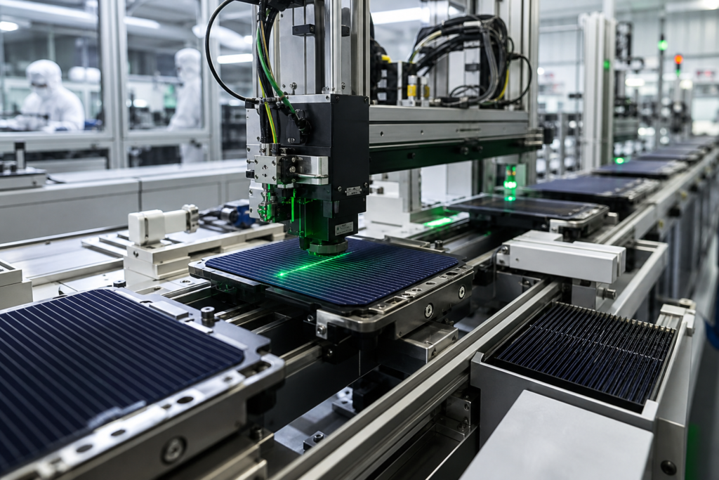
The fastest way to lose trust in a green picosecond recommendation is to pretend it solves every laser step on a BC or TOPCon hybrid line. It does not.
| Station need | Prefer | Why green picosecond is or is not the fit |
|---|---|---|
| AlOx/SiNx-class dielectric / membrane grooving at production UPH | Green picosecond (~532 nm, ~10 ps) | Absorption match + cold open + industrial average power |
| Ultra-thin a-Si:H / highly temperature-fragile HJT-like patterning | UV picosecond (~355 nm) | Stronger confinement; green may be under-protective on the most fragile films |
| Thick glass / high-energy brittle percussion on sister tools | IR picosecond (~1064 nm) | Multi-millijoule energy and glass process heritage; wrong default for thin dielectric open |
| Melt-assisted doping, LECO-style contact work, intentional thermal steps | Nanosecond / hybrid thermal lasers | Cold picosecond is the wrong physics family |
Separate grooving from laser doping in documentation. Selective-emitter or PSG-related steps may sit next to grooving on a TOPCon or BC-adjacent flow, but doping often wants controlled melt and a different metrology suite. Forcing one green picosecond chassis to fake every thermal job creates a tool that is mediocre at both.
Also separate grooving from P1–P3 thin-film solar scribing language when the stack is CIGS or similar. Those flows can use 532 nm or 1064 nm picosecond pulses for different scribes, but BC crystalline-silicon dielectric grooving has its own passivation constraints. Borrow fluence discipline from thin-film practice; do not copy the acceptance tests blindly.
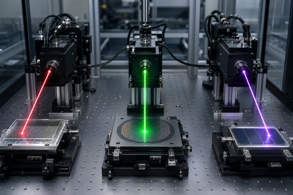
Laserion does not sell the BC cell architecture. For integrators placing sources on PV stations, these bands map cleanly to common jobs with confirmed specs only:
| PV / BC-related station | Function needed | Laserion series | Specs that matter on the RFQ |
|---|---|---|---|
| BC / PERC-class backside dielectric grooving | Selective AlOx/SiNx open without Si melt damage | Green picosecond | 532 nm; ≥120 W; ~10 ps; >300 µJ; M² <1.3; RMS ≤0.8%; Burst Mode if the recipe needs it |
| TCO / fine transparent-conductor patterning | Clean lines; lower microcrack risk than ns thermal opens | Green picosecond | Same band; DOE-ready spot uniformity for pattern fidelity |
| Thermal-fragile fine open / polymer-adjacent micro features on the tool family | Higher UV absorption; tight focus | UV picosecond | 355 nm; ≥40 W; ~10 ps; M² <1.2; RMS ≤1% |
| Wafer scribing / high-energy IR brittle work on sister tools | Deep or high-energy picosecond process | Infrared picosecond | 1064 nm; >100 W (up to ~300 W class); ≥3.5 mJ; ~10 ps; PSO |
Use the table to place green picosecond where BC grooving actually lives. Sister stations can share a vendor without sharing a wavelength—and that dual-source clarity is part of why pure-source supply helps integrators more than a locked turnkey black box.
Once wavelength and pulse class are chosen, the RFQ still fails if it only says “532 nm picosecond, high power.” Production grooving needs a short, enforceable list:
That list is how green picosecond stops being a brochure phrase and becomes a station you can FAT. It is also how procurement avoids buying ultraviolet over-spec or infrared under-selectivity because the scorecard never named the real failure modes.
If your BC rear stack is dielectric or passivation membrane grooving and the UPH model is tight, qualify a 532 nm green picosecond source near film threshold with ≥120 W-class average power and RMS/M² acceptance.
If the critical layer is a-Si:H or another ultra-fragile film, prioritize UV picosecond and accept the power and scanner-count trade.
If the dominant failure mode is incomplete open that becomes contact resistance, do not “add infrared power” first—fix absorption and fluence at the correct wavelength.
If procurement pushes nanosecond for price, put lifetime recovery, wet-clean cost, and scrap bins into the model before award.
If the process step is melt doping or contact sintering, choose a thermal laser family. Do not stretch cold grooving physics to cover a hot job.
If you already own process IP and scanners, buy a pure laser source and dual-source the wavelength band. If you need a turnkey BC cell, buy a tool OEM—and still write source-level grooving specs so quality is not trapped in an opaque module.
Before you freeze a green picosecond laser for BC solar cell grooving, write four artifacts: the stack, the open geometry, the passivation metric that defines pass/fail, and the UPH target at that quality. Ask each shortlisted source for energy-versus-repetition-rate curves at 532 nm, M² and RMS at operating duty cycle, and a written statement of whether Burst Mode is inside the frozen recipe. Those details decide whether green is a real production answer or only a coupon story.
If you’re qualifying an ultrafast source for production or integrating one into OEM equipment, talking to an applications team directly can surface stability, customization, and delivery details no product listing will tell you.
Talk to our applications team →
BC grooving rewards the wavelength that matches the film you must remove and the pulse width that protects the passivation you must keep. The process engineer who stepped back from ultraviolet-for-everything did not settle for a weaker laser. They chose the production-shaped answer for that dielectric open: green picosecond power where the stack absorbs, cold enough to defend lifetime, and strong enough to defend the line schedule.
Use a green picosecond laser for BC solar cell grooving when 532 nm selective dielectric open and industrial line speed must coexist—without paying a UV over-spec tax or an IR substrate-damage tax.
Because many BC rear jobs are selective dielectric or passivation opens where ~532 nm couples into the film stack efficiently, while ~10 ps pulses limit heat-affected damage to the silicon. Industrial green sources also supply the average power needed for production wafers-per-hour at a fluence that still protects passivation.
No. Ultraviolet is often preferred for ultra-thin, temperature-fragile layers such as a-Si:H. For AlOx/SiNx-class membrane grooving at high throughput, green picosecond can be the better station choice because it balances selective open quality with industrial average power.
Infrared can penetrate more deeply and narrow the window between clearing the dielectric and damaging silicon. Green typically weights optical energy into the films being grooved, which helps selective open when the stack is designed for that absorption. Infrared remains valuable on sister tools that need high pulse energy for glass or other brittle work.
It can look cheaper on capital expenditure. Thermal edge damage, wet recovery, lifetime loss, and scrap often erase that advantage once the cell efficiency distribution is included. Score total cost of the station, not only the laser list price.
Wavelength in the 532 nm class, pulse width around 10 ps, average power sized to wafers-per-hour at pass-fail quality (often ≥120 W class), pulse energy at the operating repetition rate, beam quality (M²), power stability (RMS), and Burst Mode only if the frozen recipe uses subpulse packets.
No. Burst Mode helps when the qualified process uses controlled subpulse packets. If the recipe runs single-pulse or simple repetition-rate operation, unused burst configuration adds integration complexity and change-order risk without improving yield.
The same 532 nm picosecond band is commonly discussed for TCO patterning and for process flows adjacent to selective-emitter work. Keep the acceptance tests separate. Membrane grooving is judged by dielectric clear and passivation retention; melt-assisted doping is judged by dopant profile and contact resistivity.
If you already own process IP, scanners, and metrology, buying a pure laser source preserves dual-source flexibility on the wavelength band. If you need a turnkey cell, buy from a tool OEM—and still write explicit source-level grooving specifications so open quality and stability are not hidden inside a black-box module.