
Most solar capacity ramps do not stall because someone forgot what a selective emitter is. They stall because the laser source that looked perfect on a coupon cannot hold the same process window when the line moves from pilot takt to GW cadence.
“When we mapped a second GW string, the first RFQ asked for femtosecond ‘to protect every stack.’ Sample coupons looked clean, but takt math failed: tool CapEx and scan strategy could not hold ~1 s/wafer class contact-open throughput without stacking more heads than the bay allowed. We re-qualified an industrial green picosecond source in the 10–120 W band for dielectric open and kept IR picosecond for thicker workhorse steps. On the sensitive a-Si:H / TCO trials we still reserved ultrafast only where HAZ budgets forced it. After two weeks of window locks, contact-open yield held while we dropped one over-specified fs head from the line plan. Scaling the solar line meant scaling a pulse class we could keep inside the process window at volume—not the shortest pulse on the datasheet.” — Process engineer, PERC+/TOPCon laser contact-open and selective-ablation qualification
That scene is why we treat “how do you scale ultrafast laser sources for high-volume solar manufacturing” as a source-and-window problem first, and a cell-architecture story second. Laserion supplies industrial ultrafast sources for integrators and production tools—not turnkey cell lines—so the practical question is which pulse class, wavelength, and stability band you can dual-source and keep inside fluence tolerance shift after shift.
To scale ultrafast laser sources for high-volume solar manufacturing, lock each laser station to a pulse class and wavelength that holds the process window at target takt, then qualify sources on 7×24 power stability, beam quality, and deliverable capacity—not peak power alone. Industrial green and IR picosecond sources cover most PERC/TOPCon dielectric open, selective emitter, TCO, and wafer-scribe work; reserve femtosecond for stacks where heat-affected zone (HAZ) budgets leave no margin; use green nanosecond where the thermal budget and cost model allow. Scaling the line means scaling sources you can integrate, spare, and keep in window—not shortening every pulse “to be safe.”
PERC-era contact open already taught the industry that laser stations are takt-critical: industry-typical recipes talk about roughly one-second-class wafer handling and tens of meters per second of scan length when dielectric openings are dense. TOPCon, HJT, and back-contact (BC) stacks raise the stakes. Passivation stacks get thinner and more temperature-sensitive. Procurement still scores vendors on $/W and pulse width. Integrators still get scored on peak power in the first RFQ column.
We see the same failure mode across qualifications: a source wins the paper compare, then drifts after thermal soak; or a femtosecond head wins the damage audit and loses the CapEx/head-count audit. R&D and procurement pull in opposite directions—one wants more average watts, the other wants the lowest unit price—while the binding constraint is often wavelength fit plus how many qualified sources arrive before the capacity gate.
If you are dual-sourcing a laser station for a second GW block, or an OEM locking a BOM for the next tool generation, the search behind this title is really: which ultrafast laser source for PV production lines can I scale without reopening the entire process window?
Start with the station list, not the laser brochure. For crystalline-silicon volume lines, the recurring laser jobs look like this:
Only after that list is frozen should you ask what must be “cold” (picosecond/femtosecond with minimal HAZ) versus what can tolerate nanosecond thermal budgets. The common mistake is buying one ultra-premium pulse class for every head so the RFQ looks consistent. Consistency on paper is not consistency on takt.
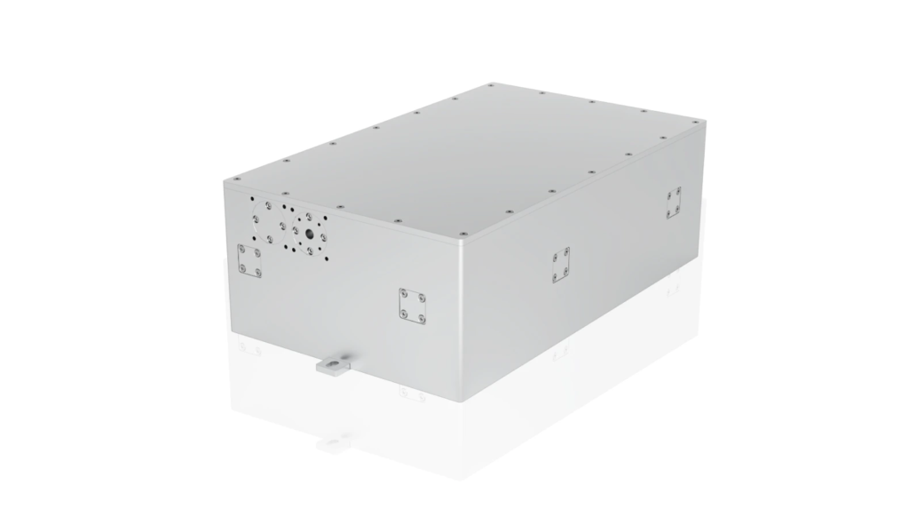
Femtosecond versus picosecond is a real decision—but it is a station decision.
Nanosecond sources deposit energy on timescales where lattice heating and melt-assisted effects are available on purpose (doping, some film scribes). Picosecond sources shrink diffusion enough for selective dielectric and TCO work while remaining industrially affordable at high average power. Femtosecond sources further confine energy for brittle or multilayer stacks that fail when HAZ creeps into passivation.
In high-volume solar, the over-spec trap is clear: specifying femtosecond everywhere protects coupons and breaks bay layout. Keep IR femtosecond (for Laserion: 1030 nm, ≥50 W, 500 fs–10 ps, pulse energy ≥1 mJ, M² ≤1.3, RMS <0.8%) for stations that truly need cold machining and sub-micron edge quality. Put industrial green and IR picosecond on the volume dielectric and scribe stations where scan speed and stability decide whether the second string turns on.
If your next sample run is already booked, confirming pulse class against the stack cross-section now—before the CapEx committee freezes head count—saves a second qualification loop later.
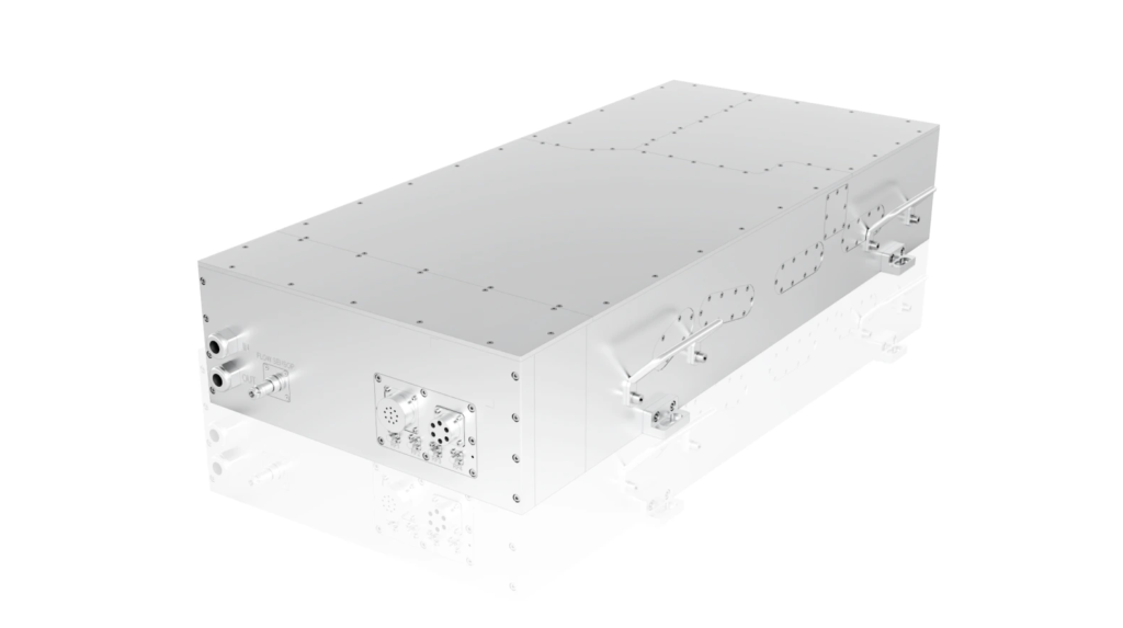
Integrators learn this the expensive way:
“Integrators get scored on peak power and pulse width in the first scorecard. On a dual-lane TOPCon tool we shipped, the higher-peak source won paper comparison—then drifted outside the ablation window after thermal soak on 7×24 duty. Scrap clustered as intermittent under-open and local damage, not as a clean ‘power too low’ signature. We switched the qualification gate to RMS power stability, M² hold, and shift-to-shift fluence repeatability under the same scan recipe, with a pure source OEM that could dual-feed spares without forcing a turnkey machine lock-in. Peak power still mattered, but it stopped being the scale metric. What scaled the line was a source that stayed inside ±window after 72-hour soak, so our OEM customers did not re-qualify optics every time volume stepped up.” — Equipment integrator OEM lead, TOPCon laser station dual-source scale-up
When you scale ultrafast laser sources for high-volume solar manufacturing, put soak tests and RMS stability in the same gate as M². Laserion’s industrial picosecond and femtosecond machining sources target RMS power stability at or below 0.8% (UV picosecond ≤1%; green nanosecond <1.5%). Those numbers are not marketing decoration—they are the difference between a locked open width and a night-shift scrap cluster that never shows up in a single-point peak-power cell.
Also score control interfaces you actually use on the tool (GATE, TRIG, PSO where the scan strategy needs position-synchronized output). A modular source that field teams can maintain matters more at GW scale than another 5% of brochure peak power you cannot hold after warm-up.
Average power still matters for ablation rate—but absorption and process margin often bind first.
“R&D wanted ‘more average watts’ to hit the next GW block; procurement wanted the lowest $/W. Both missed the binding constraint: green picosecond absorption and process margin on the dielectric stack, plus how many qualified sources we could actually take delivery of before the capacity gate. We ran a split trial—higher IR watts versus a green picosecond source in the industrial 10–120 W class matched to open/ablation absorption. Green held the open width and damage criteria at the target scan speed with less compensatory over-fluence. Procurement then scored vendors on confirmed delivery slots and field-replaceable module lead time, not only unit price. The counter-intuitive part for the steering committee: scaling ultrafast for solar was a wavelength-plus-supply problem before it was a raw-watt problem.” — R&D technical lead with procurement, green picosecond source approval for PV volume ramp
For dielectric open, SE/PSG work, and many TCO pattern steps, 532 nm picosecond is the usual industrial workhorse because photon energy and absorption improve margin versus forcing IR fluence upward until the silicon or passivation complains. For wafer scribing and thicker brittle work, 1064 nm picosecond at high average power remains the throughput path. For HJT film scribing where the cost model rejects ultrafast on every head, green nanosecond stays in the toolkit.
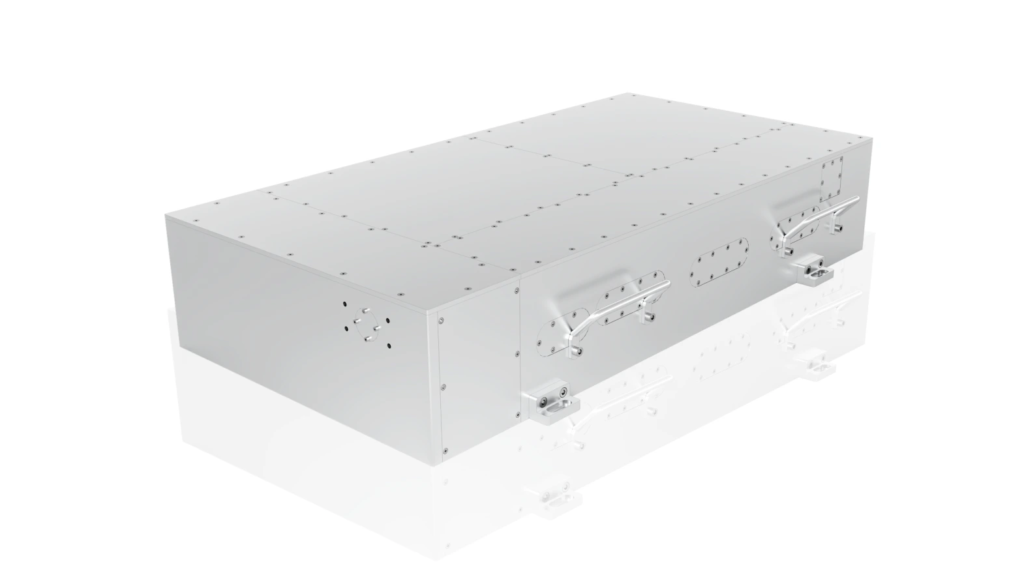
A locked recipe with a single long-lead source is not a scaled line. Ask for:
Laserion’s positioning is intentional here: pure source OEM for equipment integrators and production tools. We do not sell competing turnkey solar machines. That boundary keeps the commercial model aligned with how GW lines actually buy—tool builders integrate scanners, stages, and process IP; the source must be stable, documentable, and replaceable.
Use this as a qualification shortlist—not a claim that one source runs an entire fab. Specs are series-level from Laserion product data; final process windows still need your stack and scan recipe.
| PV / process station | Function needed | Laserion series | Specs that matter for scale |
|---|---|---|---|
| Backside membrane / dielectric grooving | Selective AlOx/SiNx open without damaging Si | Green picosecond | 532 nm; ≥120 W; ~10 ps; M² <1.3; RMS ≤0.8%; Burst Mode; DOE-ready pointing/spot uniformity |
| Laser doping (SE) | Selective PSG ablation / localized re-doping support | Green picosecond | Same band; programmable burst for energy deposition control |
| TCO patterning (ITO/FTO) | Fine lines with low microcrack risk vs ns thermal damage | Green picosecond (UV picosecond if stack demands shorter λ) | Green: ≥120 W, ~10 ps; UV ps option: 355 nm, ≥40 W, M² <1.2, RMS ≤1% |
| PV silicon wafer scribing | Throughput scribe with industrial beam quality | IR picosecond | 1064 nm; >100 W (up to ~300 W class); ≥3.5 mJ; ~10 ps; M² <1.3; RMS ≤0.8%; PSO / GATE / TRIG |
| HJT film scribing (cost-sensitive heads) | Film scribe where ultrafast is over-spec | Green nanosecond | 532 nm; >60 W @ 50 kHz; <30 ns @ 50 kHz; M² <1.2; RMS <1.5%; life >10,000 h |
| Cold solar-cell scribing / extreme HAZ stacks | True cold machining when ps margin is gone | IR femtosecond | 1030 nm; ≥50 W; 500 fs–10 ps; ≥1 mJ; M² ≤1.3; RMS <0.8% |
That table is how we want readers to meet the product line: station first, series second, confirmed numbers third.
| Wrong scale metric | Better scale metric |
|---|---|
| Shortest pulse on every head | Pulse class matched to HAZ budget and takt |
| Highest peak power on the RFQ | RMS stability + M² hold after soak |
| Lowest $/W alone | $/good wafer including scrap and re-qualification |
| One exotic source, 40-week lead | Deliverable dual-feed capacity before capacity gate |
If your station is AlOx/SiNx open, SE/PSG, or TCO patterning at GW takt, start with an industrial green picosecond source in the ≥120 W band and lock burst/fluence before you debate femtosecond.
If your station is silicon wafer scribing or other high-energy IR workhorse steps, qualify IR picosecond on average power, pulse energy, M², and PSO/trigger behavior under your scan head—not on a single peak-power screenshot.
If HJT film scribing economics cannot carry ultrafast on every tool, keep green nanosecond in the model and prove edge/damage criteria explicitly.
If—and only if—passivation or multilayer stacks fail inside a picosecond window, move that head to IR femtosecond (≥50 W class) and do not copy that choice across the whole line.
If you are an integrator, add a hard gate: 72-hour soak, RMS/M² hold, spare-feed plan from a pure source OEM. If any gate fails, you have not scaled the source—you have scaled risk.
Before you freeze the BOM for the next GW string, confirm pulse class per station, green versus IR absorption on the real stack, RMS stability under duty cycle, M² at the scan head, Burst Mode or PSO needs, and delivery slots that match tool ship dates. If you’re qualifying an ultrafast source for production or integrating one into OEM solar equipment, talking to an applications team directly can surface stability, customization, and delivery details no product listing will tell you.
Talk to our applications team →
High-volume solar does not reward the most impressive pulse on a datasheet. It rewards sources that stay inside a process window when takt, soak, and spare logistics get real. The process engineer who dropped an over-specified femtosecond head was not lowering the science bar—they were raising the scale bar. You scale ultrafast laser sources for high-volume solar manufacturing by matching pulse class and wavelength to each station, then dual-sourcing industrial sources that hold stability and delivery at GW cadence—not by shortening every pulse or chasing peak power alone.
How do you scale ultrafast laser sources for high-volume solar manufacturing without over-specifying femtosecond?
Map each station’s HAZ budget and takt first. Use industrial green/IR picosecond for most dielectric open, SE, TCO, and wafer-scribe volume work; reserve femtosecond for stacks that fail inside a picosecond window. Over-specifying femtosecond on every head raises CapEx and head count before it raises good-wafer output.
Is a green picosecond laser better than IR for PERC/TOPCon dielectric open?
Often yes for AlOx/SiNx-class open and related selective steps, because 532 nm absorption can improve process margin versus forcing IR fluence higher. Laserion’s green picosecond series is specified at 532 nm, ≥120 W, ~10 ps, with Burst Mode for energy-deposition control. Final choice still needs your stack coupons and scan recipe.
What Laserion source fits PV silicon wafer scribing?
An industrial IR picosecond source is the usual workhorse: Laserion specifies 1064 nm, >100 W (up to ~300 W class), ≥3.5 mJ, ~10 ps, M² <1.3, RMS ≤0.8%, with GATE/TRIG/PSO for tool integration. Qualify under your scribe speed and fracture criteria, not brochure peak power alone.
When is green nanosecond still right on a solar line?
When the thermal budget and cost model allow—commonly HJT film scribing and other stations where ultrafast does not pay back. Laserion’s green nanosecond series offers >60 W @ 50 kHz, <30 ns @ 50 kHz, M² <1.2, and industrial lifetime targets >10,000 hours. Prove damage and edge metrics explicitly before calling ultrafast “required.”
What should integrators test beyond peak power?
Soak the source under 7×24-like duty, then check RMS power stability, M² hold, and fluence repeatability with the production scan recipe. Also verify trigger/PSO behavior and spare-module logistics. Peak power that drifts out of window after warm-up creates scrap that never appears in the RFQ spreadsheet.
Does Laserion sell complete solar manufacturing machines?
No. Laserion is a pure laser source OEM. We supply industrial ultrafast and nanosecond sources for equipment integrators and production tools, and we partner on process-fit and delivery rather than competing with turnkey cell-line builders.
How does Burst Mode help high-volume PV laser stations?
Programmable burst control lets you set pulses per burst, timing, and energy distribution so material is removed with less waste heat accumulation than poorly tuned high-overlap pulsing. On Laserion’s green picosecond platform, Burst Mode is intended for finer energy-deposition control during dielectric and related micromachining—not as a substitute for choosing the wrong wavelength.
What if our stack needs colder processing than picosecond can hold?
Escalate that station only—typically to an IR femtosecond source (Laserion: 1030 nm, ≥50 W, 500 fs–10 ps, ≥1 mJ, M² ≤1.3, RMS <0.8%)—and keep volume heads on the industrial picosecond band. Scaling means selective cold processing, not a full-line femtosecond mandate.