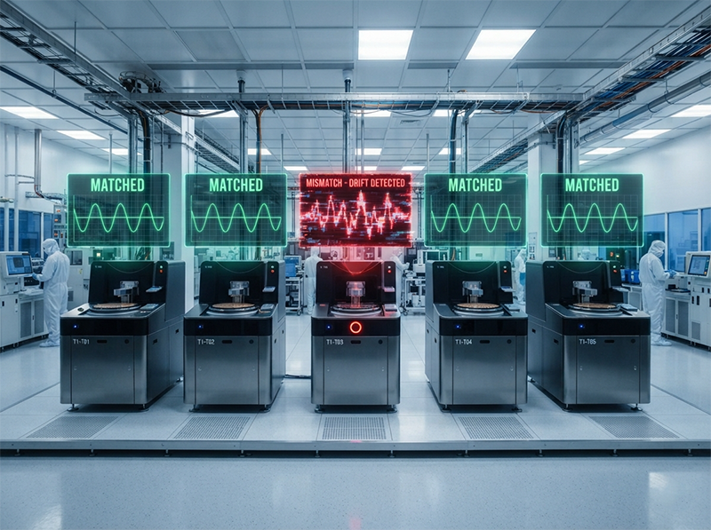
We’ve all heard the story. A new multi-billion dollar fab is ramping up, with two production lines—one in Arizona, one in Taiwan—using supposedly identical, top-of-the-line metrology tools. Yet, they can’t get the data to match. The same reference wafer, measured on these “identical” machines, yields a critical dimension (CD) discrepancy of just 0.1 nanometers. It sounds trivial, but it’s enough to break global yield models and throw a wrench in a synchronized, worldwide production ramp.
For weeks, engineers might blame the software, the robotics, anything but the core measurement physics. This isn’t a hypothetical; it’s the daily reality for process integration leaders trying to manage a global fleet of capital equipment. The root cause is often buried in a component that’s taken for granted.
“We were qualifying two new scatterometry (OCD) tools for our 3nm FinFET ramp…After weeks of blaming the software and mechanics, we found the root cause: the ‘standard’ laser sources. Their center wavelength drifted by just 5 picometers over an 8-hour shift, but they drifted differently. The tool using a truly stabilized, narrow-linewidth DFB laser with <0.1nm linewidth didn’t have this problem… We weren’t just buying higher precision; we were buying inter-tool authority. The final decision wasn’t just about a source that could measure 0.1nm, but one that ensures 0.1nm means the exact same thing in Arizona today and in Taiwan six months from now.”
— Head of Process Integration, qualifying a global fleet of metrology tools
This insight is profoundly important. It elevates the choice of a laser source from a technical line item to a strategic decision about global operational control. The challenge in advanced semiconductor manufacturing isn’t just measuring at the sub-nanometer level; it’s ensuring that measurement is an absolute, transferable authority, not a local, variable opinion.
In semiconductor inspection, a narrow-linewidth laser source is critical not just for its inherent precision, but for the stability and consistency of that precision over time, across temperatures, and between different tools. This stability transforms the measurement from a variable into a constant, solving the multi-million dollar “tool-to-tool matching” problem, reducing the total cost of ownership for equipment OEMs, and preventing false production shutdowns caused by unreliable metrology data.
As the industry pushes beyond 3nm nodes, the physics of manufacturing has become unforgiving. The value of a single, fully processed 300mm wafer can exceed that of a luxury car, and a new fabrication plant represents a $20+ billion investment. In this environment, any source of variation is an existential threat to profitability. The traditional focus has been on improving the process tools themselves, but we’ve reached a point where the ability to trust the measurement is the primary bottleneck.
Our experience across dozens of metrology tool integrations shows that fabs are no longer just asking “How precise is your tool?” They are asking, “How consistent is that precision across 50 tools, 3 continents, and a 5-year operational lifespan?” Answering this question forces a shift in focus from the measurement tool’s software to the fundamental stability of its core components.
This article will break down why a truly stable, narrow-linewidth laser source is no longer a “nice-to-have” technical specification. It has become the foundational enabler of scalable, profitable, next-generation semiconductor manufacturing. We will explore this from the perspective of the fab director managing a global fleet, the OEM building the tool, and the engineer on the front lines of yield management.
The biggest challenge in a modern fab is not making one perfect chip; it’s making 10 million identical chips across a global fleet of machines. The “Tool Matching” or “Fleet Management” problem is at the heart of this.
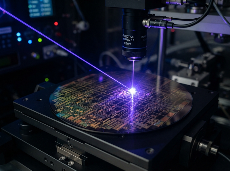
Optical Critical Dimension (OCD) or scatterometry tools work by shining light of a very specific color (wavelength) onto the nanoscopic structures of a wafer. They then measure the pattern of the reflected light and use a complex model to reconstruct the 3D shape of those structures. If the wavelength of the light source drifts, even by a few picometers, the “ruler” itself has changed. The model will report a change in the wafer’s dimension, even if the wafer is perfect.
When a fab uses dozens of these tools, each with a “standard” laser source that has its own unique thermal drift characteristics, the result is a fleet of tools that can never agree. This is the scenario described by the Process Integration Director. To solve it, engineering teams are forced into creating complex, machine-specific “offset” or “correction” algorithms—a brittle and operationally disastrous workaround.
A truly stabilized, narrow-linewidth source attacks the problem at its physical root.
| Feature | Standard “Narrow” Source | Thermally Stabilized Narrow-Linewidth Source | Impact on Fleet Management |
|---|---|---|---|
| Wavelength Stability | Drifts with temperature & time | Locked to a physical constant | All tools use the exact same “ruler.” |
| Linewidth | <1 nm (on paper, at 25°C) | <0.1 nm (guaranteed across operating range) | Reduces model uncertainty in OCD. |
| Tool Matching Result | Requires constant software correction | Achieved at the hardware level | Radically simplifies fleet management. |
| Operational Impact | “Chasing ghosts,” divergent yield models | A single source of truth for global ops | Faster fab ramps, transferable processes. |
Investing in a source that guarantees wavelength stability is a direct investment in operational simplicity and scalable growth.
If your teams are spending more time matching tools than improving processes, it’s time to inspect your light source specifications.
For an Original Equipment Manufacturer (OEM) building a metrology platform, the pressure to reduce the Bill of Materials (BOM) cost is immense. It’s tempting to select a laser source that meets the minimum required linewidth on paper and costs 15% less. This decision often proves to be a catastrophic financial miscalculation.
The R&D Lead’s story is a classic case study in Total Cost of Ownership (TCO). A laser source doesn’t operate on a clean lab bench at 25°C; it lives inside a dense, heat-generating machine where ambient temperatures can easily reach 35-40°C. Many lower-cost sources achieve their narrow linewidth under ideal conditions, but their performance degrades unpredictably as temperature fluctuates. The linewidth broadens, the center wavelength drifts, and the tool’s reliability collapses.
For the OEM, the consequences are severe:
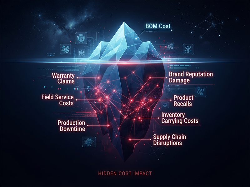
A high-performance, thermally-insensitive laser source is not a cost; it is an insurance policy. By guaranteeing performance across the full operational range, it protects the OEM’s profit margins, brand reputation, and innovation capacity. A $5,000 annual reduction in service cost per machine, as the R&D lead estimated, makes the upfront investment in a superior source the only logical financial choice.
The most dangerous tool on a production line is one that gives you a precise, but incorrect, answer. This is the nightmare scenario for a Yield Engineer.
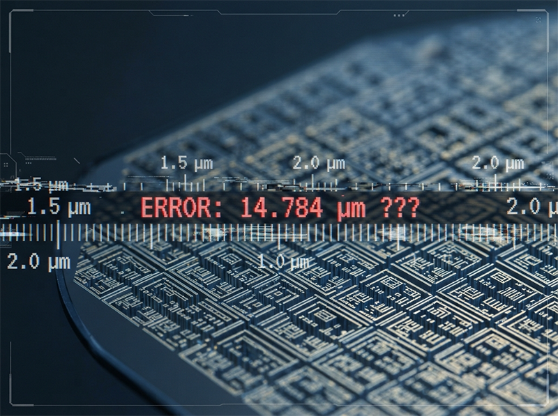
As described in the story of the SiC fab, a 3% yield excursion triggered a multi-day, multi-million dollar investigation. The entire team, trusting their metrology data, focused on the etch process chamber. They were hunting a ghost. The actual problem was that the laser source inside the OCD tool, after hours of continuous operation, experienced a “mode hop.”
Mode-hopping is a phenomenon where the laser’s output frequency jumps abruptly, like a radio station suddenly changing its channel. To the OCD system, this looks identical to a change in the wafer’s diffraction pattern. The tool reported a process drift when, in reality, the wafer was fine—the ruler itself had glitched.
This creates a crisis of confidence. If engineers cannot trust their metrology, the entire foundation of modern process control (and the billions invested in it) begins to crumble. The solution is to use sources that are not just “narrow-linewidth,” but are guaranteed single-frequency and mode-hop-free over their entire operational life. This isn’t a minor feature; it is the fundamental requirement for building a trustworthy measurement system.
Your role determines how you view the light source, but the conclusion is the same: stability is a strategic imperative.
A datasheet can tell you a laser’s linewidth under ideal conditions. It cannot tell you how that laser will behave after 10,000 hours of continuous operation inside a hot, vibrating machine. Long-term stability, thermal insensitivity, and guaranteed mode-hop-free operation are characteristics that are only revealed through rigorous, extended testing. These are the specifications that truly determine a source’s value in a production environment.
If you’re sourcing at scale, talking to a supplier directly can surface details no product listing will tell you.
We began with the challenge of making 0.1nm mean the same thing everywhere in the world. The solution lies in understanding that a laser source in a metrology tool is not just an illuminator; it is the physical embodiment of your standard of measurement. Its stability is a direct proxy for the stability of your data, the consistency of your global operations, and the trustworthiness of your entire yield management strategy.
In semiconductor manufacturing, a stable photon is the ultimate source of authority.
1. What is Optical Critical Dimension (OCD) or scatterometry?
OCD, also known as scatterometry, is a non-destructive optical metrology technique used in semiconductor manufacturing. It shines light onto the periodic structures of a wafer and measures the properties of the reflected light. By comparing this “signature” to a complex physics-based model, it can accurately reconstruct nanometer-scale 3D features like FinFETs and DRAM capacitors.
2. Why is “tool matching” so difficult and expensive?
Tool matching is difficult because modern semiconductor features are so small that even tiny variations in the measurement tool’s components (like laser wavelength drift due to temperature) can cause significant measurement discrepancies. This forces fabs to spend enormous amounts of engineering time creating custom correction algorithms for each tool to ensure the entire “fleet” produces consistent data, a costly and inefficient process.
3. What is laser ‘mode-hopping’ and why is it bad for inspection?
Mode-hopping is an abrupt, random jump in a laser’s wavelength. For an OCD tool that relies on a stable wavelength as its “ruler,” a mode hop is catastrophic. It creates a sudden, false change in the measurement data, leading engineers to believe there is a problem with the manufacturing process when, in fact, the measurement tool itself has failed. This can lead to unnecessary and expensive production shutdowns.
4. How does a narrow linewidth help in OCD measurements?
In scatterometry, the reflected light’s signature is highly dependent on wavelength. A narrower laser linewidth means the light used is more “monochromatic” or spectrally pure. This reduces ambiguity in the optical model, allowing for a more accurate and repeatable reconstruction of the wafer’s features. It sharpens the “ruler,” making the measurement more precise.
5. What does the Total Cost of Ownership (TCO) for a laser source include?
TCO for a laser source goes far beyond its initial purchase price (BOM cost). It includes the high costs of field service calls, repairs, and recalibration if the source is unstable. It also includes the massive financial impact of production downtime and the damage to an OEM’s brand reputation caused by unreliable equipment—all of which often trace back to a “low-cost” but unstable source.
6. How does temperature affect a laser source’s stability?
Most laser sources are sensitive to temperature. As the temperature inside a machine changes, the laser cavity can expand or contract, causing its center wavelength to drift and its linewidth to broaden. A high-performance, “thermally-insensitive” source uses advanced optical design and thermal management (like integrated thermoelectric coolers and fiber Bragg gratings) to maintain its performance across a wide operating temperature range.
[1] Bischoff, J., et al. (2012). Optical scatterometry for process control in semiconductor manufacturing. AIP Conference Proceedings, 1496(1), 317-323. https://doi.org/10.1063/1.4766491
[2] Silver, R. M., et al. (2014). Reference metrology for the semiconductor industry. Journal of Research of the National Institute of Standards and Technology, 119, 619-631. https://doi.org/10.6028/jres.119.025
[3] Bodermann, B., et al. (2018). Towards traceable optical metrology for the semiconductor industry. Measurement Science and Technology, 29(12), 124003. https://doi.org/10.1088/1681-7575/aadf74