The first question every process engineer asks when specifying a laser source for wafer marking is: which wavelength? It feels like the safe, technically defensible starting point. Shorter wavelength means shallower photon absorption, lower thermal input, cleaner mark. UV at 355 nm is the conservative call. It passes pilot. It satisfies the initial qualification checklist. Then the line scales to 150 mm SiC wafers with tighter kerf budgets, and micro-crack density at mark edges climbs past the 50 ppm reject threshold—without a single wavelength change.
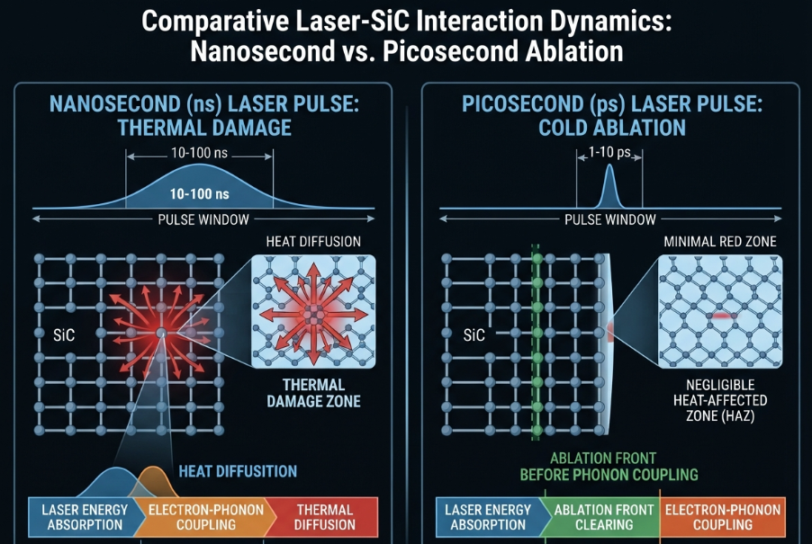
“Specifying a UV source for wafer backside marking on SiC felt like the conservative call — shorter wavelength, lower photon absorption depth, textbook ‘cold marking.’ It held through pilot. Then the line moved to 150mm SiC wafers with tighter kerf budgets, and micro-crack density at mark edges climbed past the 50 ppm reject threshold. The wavelength hadn’t changed. What the spec sheet didn’t surface was pulse duration relative to the phonon relaxation time of SiC — roughly 10–50 ps. At nanosecond pulse widths, electron-phonon coupling completes within the pulse, depositing thermal energy into the lattice before the ablation front clears. Switching to a 10 ps source held HAZ under 5 µm at the same 355 nm equivalent fluence, and micro-crack rejects dropped below 8 ppm. The variable the team had been optimising — wavelength — was not the one setting the damage floor.”
— process engineer, SiC wafer backside marking line qualification, 150 mm node
This is not an edge case. Across SiC, GaN, and sapphire substrates, the same mismatch between assumed and actual damage-driving parameters surfaces repeatedly. The variable engineers spend months optimizing is frequently not the one setting the yield floor.
The laser source parameters that most directly determine wafer marking quality and throughput are pulse duration relative to the substrate’s phonon relaxation time, output power stability over the full operating lifetime, and the ablation threshold fluence window. Wavelength matters, but it is not the primary determinant of HAZ or micro-crack density on wide-bandgap materials like SiC. Getting these three parameters right determines whether your line holds yield at volume—or spends weeks in re-qualification.
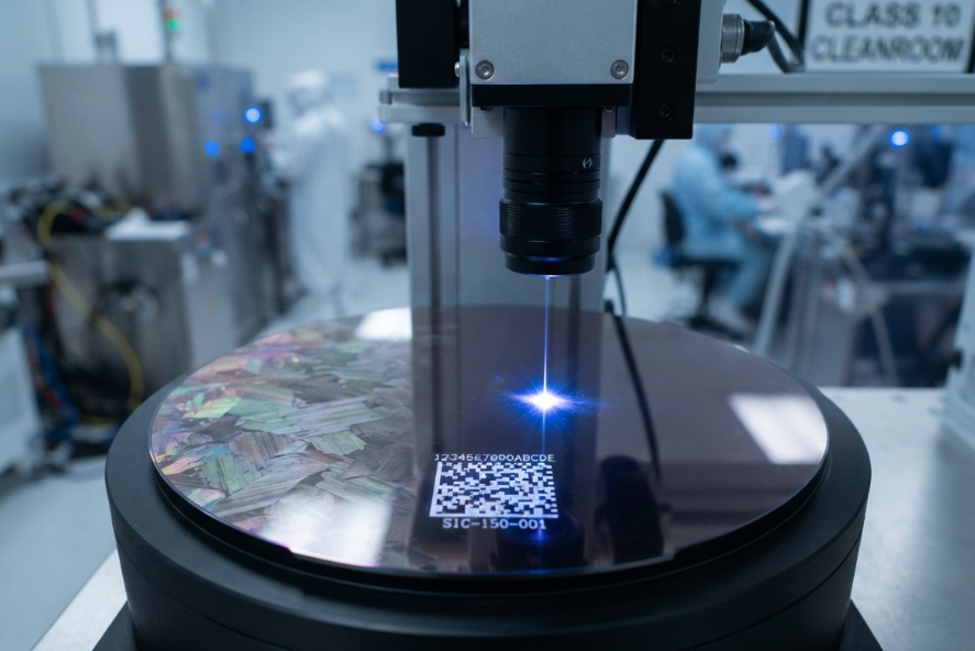
Wafer marking sits at the intersection of process physics and semiconductor economics. A Direct Part Mark (DPM)—typically a SEMI M12-compliant Data Matrix code—must be readable by automated vision systems at every stage of the fab workflow. If the mark quality drifts or edges crack, the downstream consequences are not limited to scrapped wafers. In a high-volume fab running 200 mm or 300 mm wafers, a marking-induced process change notification (PCN) triggers a full re-qualification cycle. In our experience working across fab-tool qualification projects, that re-qualification window is a minimum of 30 days of production hold, with MES traceability chains interrupted and customer delivery commitments at risk.
The reason this question is so frequently misanswered is that the spec sheets for UV laser sources are written around the parameters that are easy to measure and compare: average power, pulse energy, wavelength, and MTTF. The parameters that actually govern damage at the substrate level—pulse duration relative to phonon relaxation time, power stability over 10,000+ operating hours, and focal depth tolerance—rarely appear in competitive comparisons. This article addresses all three.
On silicon wafers, nanosecond UV lasers have a long, successful track record. The material’s phonon relaxation dynamics and ablation threshold are well-characterized at ns timescales. When fabs migrate to SiC for power devices, or to GaN for RF and LED applications[1], the same laser sources are often carried forward. This is where yield fails silently.
SiC has a phonon relaxation time of approximately 10–50 ps. This is the timescale over which excited electrons transfer their energy to the crystal lattice as heat. A standard nanosecond pulse, at 5–20 ns duration, is 100 to 2000 times longer than this window. The electron-phonon coupling process completes entirely within the pulse. By the time the ablation front clears, the lattice has already absorbed thermal energy, and the HAZ is determined by thermal diffusion—not ablation efficiency.
Switching to a 10 ps picosecond source changes the physics fundamentally. The pulse ends before electron-phonon coupling completes. Material is removed by cold ablation before heat can transfer to the surrounding lattice. At the same 355 nm equivalent fluence, this holds HAZ under 5 µm and drops micro-crack rejects from above 50 ppm to below 8 ppm. The yield improvement is not incremental—it is a physical phase transition in how the material responds.
Common Mistake: Qualifying a UV nanosecond source on silicon and assuming it transfers directly to SiC or GaN without re-evaluating pulse duration against the new substrate’s phonon relaxation time.
The implication for sourcing is direct: when a spec sheet lists wavelength and average power but not pulse duration relative to target substrate phonon dynamics, that sheet is incomplete for wide-bandgap wafer marking decisions.
The second parameter that most engineers discover late in integration is the ablation threshold fluence window—and how strongly it is governed by pulse duration. This is where the physics of the light source propagates upward into system architecture decisions.
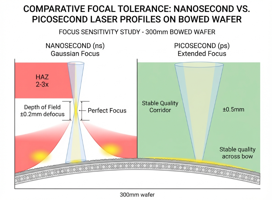
“The integration spec called for three-axis dynamic autofocus — Z-compensation across the full 300 mm field to handle wafer bow and warp. It worked. It also added six weeks of motion-control tuning, a dedicated focus sensor, and a non-trivial failure mode to the FMEA. What the system was compensating for had a source-level explanation: at nanosecond pulse durations, the ablation threshold fluence window is shallow — defocus of ±0.2 mm is enough to push the process outside the low-damage corridor, driving HAZ up by 2–3×. A picosecond source’s ablation threshold is steeper — the nonlinear intensity dependence means the process tolerates ±0.5 mm of focal shift before mark quality degrades measurably. The three-axis system solved a real problem. It solved it at the system layer because the light source made it necessary.”
— integration engineer, 300 mm wafer marking module development, fab-tool qualification
This observation carries significant engineering economics. A nanosecond UV source has a linear ablation threshold response: as fluence drops with defocus, the process exits the low-damage window smoothly and progressively[2]. A ±0.2 mm focal shift on a bowed 300 mm wafer is enough to raise HAZ by 2–3×. The engineering answer is a three-axis dynamic autofocus system with a dedicated focus sensor.
A picosecond source operates on a nonlinear intensity-dependent ablation threshold. Because material removal is driven by multiphoton ionization rather than linear absorption, the threshold is steep. The process remains within the quality window across a ±0.5 mm focal shift—more than double the nanosecond tolerance. The three-axis autofocus system is no longer necessary at the same confidence level.
| Parameter | Nanosecond UV Source | Picosecond Source |
|---|---|---|
| Focal Depth Tolerance | ±0.2 mm | ±0.5 mm |
| HAZ at Max Defocus | 2–3× baseline | Minimal degradation |
| Autofocus Requirement | Three-axis dynamic system | Simplified or single-axis |
| Integration Timeline Impact | +6 weeks motion tuning | Baseline |
| FMEA Failure Modes Added | Focus sensor + Z-motor | None additional |
Six weeks of motion-control tuning is not just an engineering inconvenience. At a fab-tool qualification node, every week of delay represents lost production capacity and deferred revenue. The source-level parameter—pulse duration—determined the system-level complexity before the first mechanical drawing was issued.
If you’re specifying a wafer marking system at scale, talking to a supplier directly at the source-selection stage can eliminate system-layer costs that won’t appear on any component quote.
The third parameter is the one most commonly reduced to a single number in competitive comparisons: MTTF. Mean time to failure tells you when the source stops working. It tells you nothing about how it performs in the 2,000 hours before it fails.
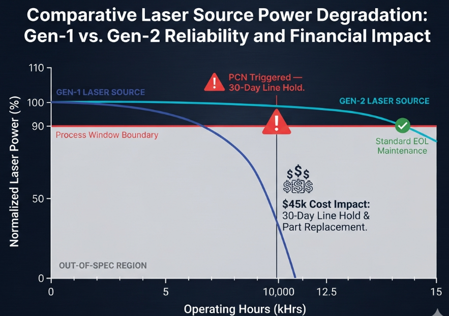
“Two UV nanosecond sources were shortlisted at a $12,000 price delta. The lower-cost unit quoted 15,000 hours MTTF. At three-shift operation that is roughly 5 years—acceptable on paper. What the comparison missed was output power stability over that curve: by hour 10,000, average power had drifted 18%. At the original process recipe, that 18% drop pushed fluence below the ablation threshold for SEMI M12-compliant mark depth. The process window had failed 1,800 hours before the source reached MTTF. Triggering a PCN and re-qualification added 30 days of line hold and re-certification costs that exceeded the original $12,000 price delta. The cost comparison that mattered was not the one on the quote sheet.”
— process technology lead, wafer ID system sourcing review, 200 mm fab expansion
This is the hidden cost structure of laser source procurement. An 18% power drift over 10,000 hours does not appear in the MTTF figure. It does not appear in the standard acceptance test. It appears when the process recipe, written for a fresh source, begins producing sub-threshold marks on wafers[3] that will be shipped to customers.
The downstream consequence in a semiconductor fab is specific and costly. SEMI M12 Data Matrix compliance is a traceability requirement, not a cosmetic one. When mark depth or contrast falls outside specification, the affected wafers cannot be released without re-inspection. If the root cause is identified as a source parameter change, a PCN is required. PCN-triggered re-qualification runs a minimum of 30 days in most fab environments, with full MES traceability chain interruption. The $12,000 price delta that drove the original sourcing decision becomes structurally irrelevant against that cost.
The correct procurement comparison is not initial price versus MTTF. It is total cost of ownership across the operating lifetime, weighted by power stability curve, re-qualification risk, and the cost per day of a line hold at your specific production volume.
To specify the right laser source for wafer marking, use this framework:
Wafer marking source selection is a decision with a long tail. The parameters that determine yield—pulse duration, focal tolerance, power stability—are frequently absent from competitive spec sheets and only surface during integration or, worse, during volume production. No product listing will tell you where your specific process recipe sits relative to the source’s power drift curve at hour 8,000. If you are sourcing at scale, talking to a supplier directly can surface details no product listing will tell you.
Three parameters—pulse duration relative to phonon relaxation time, focal depth tolerance, and output power stability over operating lifetime—determine whether a wafer marking line holds yield at volume or enters re-qualification. Wavelength is a necessary input but not a sufficient one. The engineers who discover this in pilot qualification save months of rework and hundreds of thousands in scrap and re-certification costs. The engineers who discover it in production pay a different kind of tuition. In wafer marking, the spec sheet shows you what the source can do on day one; the physics determines what it does to your yield on day 300.
Why does wavelength alone not determine HAZ in SiC wafer marking?
In wide-bandgap materials like SiC, the phonon relaxation time is approximately 10–50 ps. A nanosecond UV pulse, even at 355 nm, is 100–2000× longer than this window, meaning electron-phonon coupling completes within the pulse and deposits thermal energy into the lattice before ablation clears. Wavelength controls photon absorption depth; pulse duration controls whether heat transfers to the lattice at all.
What pulse duration is recommended for SiC wafer backside marking?
A picosecond source at approximately 10 ps or shorter is recommended for SiC. At this pulse duration, the ablation front clears before electron-phonon coupling completes, achieving cold ablation. In production qualification, a 10 ps source at 355 nm equivalent fluence has demonstrated HAZ under 5 µm and micro-crack reject rates below 8 ppm, compared to above 50 ppm on nanosecond UV sources.
How does laser pulse duration affect autofocus system requirements in 300 mm wafer marking?
Nanosecond UV sources have a shallow ablation threshold fluence window: ±0.2 mm of defocus is sufficient to raise HAZ by 2–3×, requiring three-axis dynamic autofocus with a dedicated focus sensor. Picosecond sources have a steeper, nonlinear threshold, tolerating ±0.5 mm of focal shift before mark quality degrades measurably. Selecting a picosecond source can eliminate the need for a three-axis autofocus system and remove up to six weeks from integration timelines.
What is the real cost of laser source power drift in a semiconductor fab?
When output power drifts past the process window boundary—typically 15–20% degradation—the original process recipe produces sub-threshold marks that fail SEMI M12 Data Matrix compliance. This triggers a Process Change Notification (PCN) and full re-qualification, with a minimum 30-day line hold in most fab environments. In a 200 mm fab expansion scenario, this re-qualification cost routinely exceeds the initial price delta between competing source options.
How should I compare two UV laser sources for wafer marking procurement?
Do not compare on initial price and MTTF alone. Request the output power stability curve over the full rated operating lifetime and calculate the earliest point at which power drift pushes your process recipe below the ablation threshold. Then model the re-qualification cost exposure at that trigger point against your production volume. That total cost of ownership calculation, not the quote sheet price delta, is the correct basis for the sourcing decision.
Is a femtosecond laser always better than a picosecond laser for wafer marking?
Not necessarily. For most wafer marking applications—SiC backside marking, PCB Data Matrix codes, and standard silicon ID marking—a 10 ps picosecond source provides sufficient cold ablation performance at significantly lower capital cost and higher average power throughput. Femtosecond sources carry a premium that is only justified when the material’s damage threshold is so narrow that sub-picosecond pulse durations are required to stay within it. Over-specifying to femtosecond without validating against the actual material tolerance is a common source of unnecessary capex.
What SEMI standard governs wafer marking quality requirements?
SEMI M12 defines the Data Matrix symbology and readability requirements for wafer ID marking, including mark depth, contrast, and cell geometry tolerances for automated vision system reads. When laser source power drift or mark degradation causes non-compliance with SEMI M12 specifications, a full Process Change Notification and re-qualification cycle is required before affected wafers can be released.
[1]“Wide Bandgap Power Electronics Strategic Framework”. Authoritative semiconductor-materials references identify silicon carbide as a major wide-bandgap material for high-power electronics and gallium nitride as important for radio-frequency electronics and light-emitting diodes, supporting the stated application mapping. Evidence role: general_support; source type: institution. Supports: SiC is used for power devices, while GaN is used for RF and LED applications.. Scope note: This supports the typical application domains of SiC and GaN, not the specific behavior of laser processes after fab migration.
[2]“Ultrafast Laser Pulse Interaction with Dielectric Materials”. A peer-reviewed laser-ablation study or review should substantiate that nanosecond UV ablation behavior depends on delivered fluence relative to an ablation threshold, with defocus changing spot size and surface fluence; this supports the mechanism but may not prove the exact process window for the wafer system described. Evidence role: mechanism; source type: paper. Supports: Nanosecond UV laser ablation changes progressively as defocus reduces surface fluence relative to the ablation threshold.. Scope note: Likely contextual unless the source uses the same wavelength, pulse duration, material stack, and optics.
[3]“Metal Material Processing Using Femtosecond Lasers – PMC – NIH”. Studies of laser marking and laser–material processing show that mark formation and contrast depend on delivered laser fluence, power, and process thresholds, supporting the mechanism by which reduced source output can make a previously qualified recipe produce insufficient marks. Evidence role: mechanism; source type: paper. Supports: A process recipe written for a fresh laser source can begin producing sub-threshold marks on wafers as source power drifts downward.. Scope note: The evidence would support the general processing mechanism, not prove the specific 18% drift value or a particular wafer-marking recipe.