When micro-delamination appears on the cut edge of a flex PCB, the immediate instinct of any process engineer is to dial down the pulse energy. The prevailing assumption is that protecting the delicate polyimide substrate requires the gentlest possible touch. However, this conservative approach invariably stretches cycle times and leaves a measurable heat-affected zone (HAZ). The reality is that simply lowering power is a workaround that trades yield for massive throughput losses.
To truly understand how UV lasers prevent delamination in PCB cutting, we must discard the “lower power is safer” mindset.
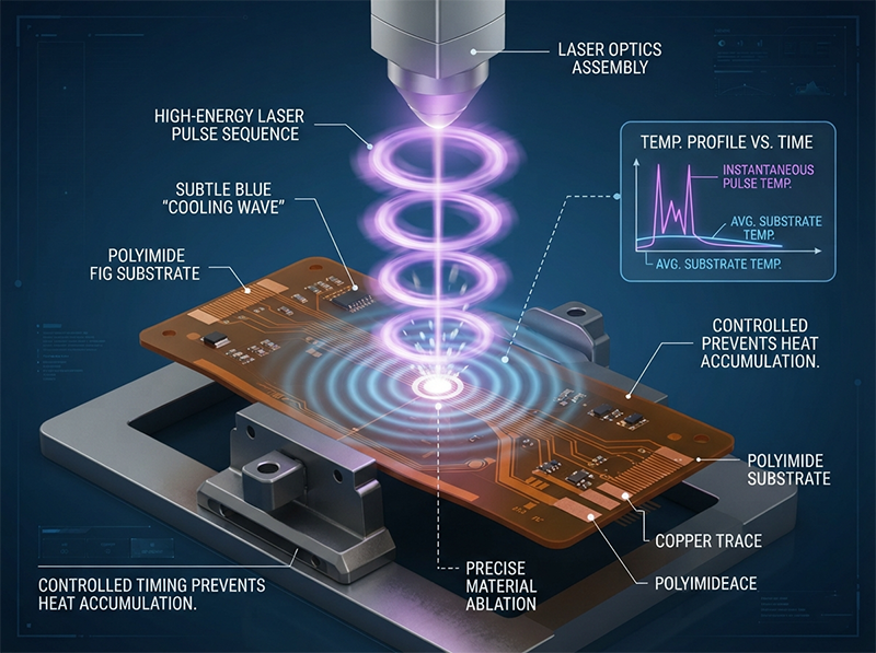
“When flex PCBs showed micro-delamination at the cut edge, the instinct was to dial down pulse energy to protect the polyimide. But lowering power just stretched cycle time and still left a measurable HAZ. Shifting to a high pulse energy UV source (~400μJ) with controlled pulse timing actually eliminated the heat buildup. On a 0.13mm FPCB, it held the HAZ to near-zero and pushed cutting speed from 11mm/s to 13mm/s. The variable preventing delamination wasn’t total energy delivered—it was spatial and temporal pulse control.”
— Process engineer, FPC singulation line qualification
This firsthand observation exposes a fundamental flaw in how we specify laser parameters. If dropping power doesn’t solve delamination, what does? The answer lies in shifting our focus from total energy delivery to precise spatial and temporal pulse control, a physics-driven approach that fundamentally changes the material interaction.
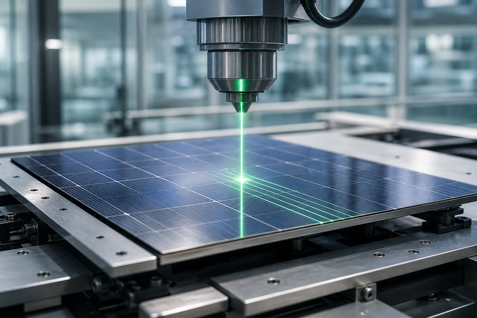
UV lasers prevent delamination in PCB cutting by combining the high photon energy of a 355nm wavelength with high single-pulse energy (around 400μJ) and controlled pulse timing. This combination forces immediate photoablation—vaporizing the material before heat can diffuse into the surrounding laminate. The key to zero delamination is not reducing power, but managing the precise interval between pulses to prevent thermal accumulation in the resin and glass fibers.
If you are qualifying a new laser system for PCB depaneling or FPC singulation, you are likely caught between two conflicting metrics: cutting speed and edge quality. Push the laser too hard, and the resin melts, causing glass fiber delamination. Slow it down to protect the board, and your cost per part skyrockets.
In our engineering practice evaluating laser systems for electronic manufacturing services (EMS) providers, we frequently see lines running at 60% capacity because engineers are terrified of edge carbonization. They purchase 355nm UV lasers knowing the wavelength is theoretically “cold,” but when they encounter PCB cutting HAZ and micro-delamination on the factory floor, their immediate response is to reduce pulse energy. This creates a hidden bottleneck that destroys Overall Equipment Effectiveness (OEE).
People searching for this answer are not just looking for a wavelength specification; they are looking for a way to guarantee zero delamination without sacrificing throughput. The true answer requires examining the physics of beam-material interaction and recognizing that relying on standard workarounds—like V-grooving on thick boards—often introduces the exact thermal damage you are trying to avoid.
The foundation of preventing delamination lies in the physics of optical absorption. The 355nm UV wavelength is highly absorbed by copper and polyimide, ensuring that energy is deposited in a very shallow depth. However, wavelength alone does not guarantee a clean cut.
The breakthrough comes from utilizing a high pulse energy UV DPSS laser PCB system[1]. Delivering approximately 400μJ of single-pulse energy creates a massive ablation pressure that instantaneously vaporizes the material. The critical factor is that this high energy must be paired with controlled pulse timing.
By precisely controlling the interval between successive pulses, the energy from the first pulse dissipates entirely before the next pulse arrives. This temporal management prevents heat from accumulating in the substrate. If the pulse interval is too short, the substrate cannot cool, and the resin melts, leading to delamination. By mastering this timing, engineers can push cutting speeds from 11mm/s to 13mm/s on 0.13mm FPCB materials while holding the HAZ to near-zero. The physics of Gaussian beam focusing dictates that high energy focused tightly creates a clean plasma, leaving no thermal residue behind.
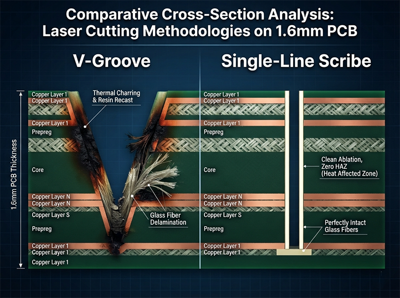
When processing thicker 1.6mm multilayer boards, the challenge compounds. Engineers often struggle to cut deep enough without the beam clipping the edge of the kerf, causing secondary thermal damage. The industry’s standard workaround is the V-groove method.
The assumption is that using lower pulse energy and making laterally displaced passes will gently scribe a wide trench without overheating the board. In practice, this method is highly destructive.
“To avoid delamination and beam clipping on 1.6mm multilayer boards, the standard approach was using low pulse energy to scribe a ‘v-groove’ with laterally displaced passes. It worked, but the repeated passes widened the kerf and thermal accumulation still caused glass fiber delamination. Switching to a ~400μJ UV DPSS laser to repeatedly scribe the exact same line—without lateral offset—delivered a narrower trench and eliminated HAZ-induced delamination entirely. The industry’s standard workaround for thick materials was actually the source of the thermal damage.”
— R&D lead, PCB equipment selection and process development
The V-groove approach forces the laser to repeatedly pass over the same general area. Even with lower pulse energy, the cumulative heat load from multiple overlapping passes causes thermal accumulation[2]. This repeated heating melts the epoxy resin, causing the glass fibers to separate.
Switching to a high-energy single-line direct scribe—repeatedly hitting the exact same line without lateral offset—fundamentally changes the thermal dynamic. The high energy ablates the material cleanly, and because the line is not widened, the beam profile does not clip the trench walls. This keeps the heat concentrated in the ablation plume, not the substrate.
| Parameter | V-Groove Method (Low Energy) | Single-Line Direct Scribe (~400μJ) |
|---|---|---|
| Pass Strategy | Multiple laterally offset passes | Repeated passes on identical line |
| Kerf Width | Wide (reduces board utilization) | Narrow (maximizes utilization) |
| Thermal Load | High (cumulative overlap heating) | Low (efficient single-track ablation) |
| Delamination Risk | High (resin melting from overlap) | Eliminated (cold ablation per pass) |
| HAZ (Heat-Affected Zone) | Clearly visible | Near-zero |
This comparison highlights a counterintuitive truth: utilizing UV laser vs V-groove thick PCB strategies shows that higher energy concentrated in a single track is thermally safer than distributing lower energy across a wider area.
Delamination is not the only yield killer caused by poor laser pulse control. Soot, debris, and edge carbonization force EMS providers to add costly post-processing steps. When sourcing teams evaluate lasers purely based on the 355nm wavelength spec sheet, they often assume “UV cold ablation” equates to a perfectly clean cut.
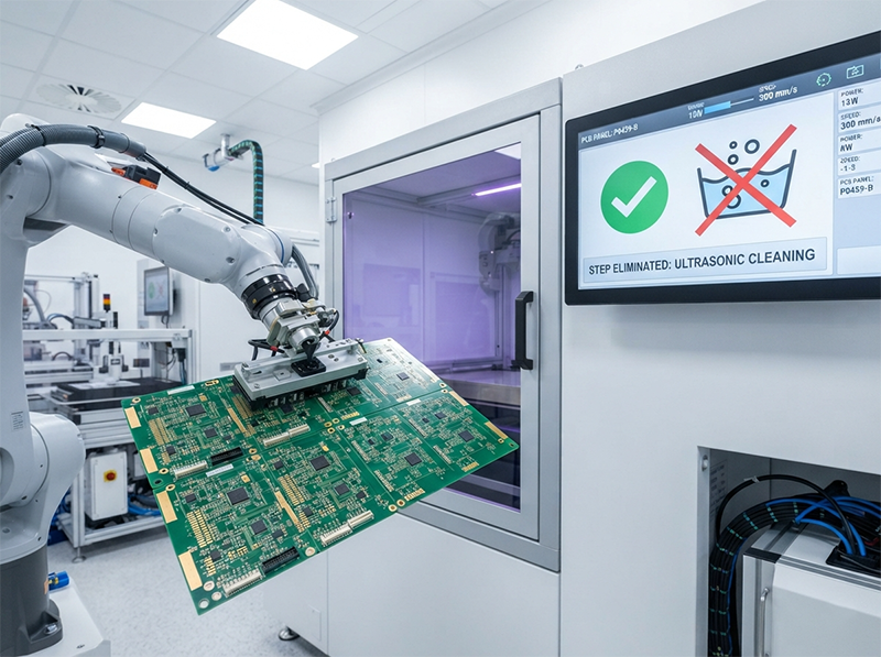
In reality, standard UV lasers lacking precise pulse timing cause micro-explosions that leave carbonized residue on low-κ dielectric boards. This debris is conductive and must be removed before downstream EMI shielding or coating. Consequently, the factory has to add an entire ultrasonic cleaning line.
The true differentiator is a high-pulse-energy UV DPSS laser with proprietary pulse control. By completely vaporizing the material without melting the resin, the cut edges emerge clean, delamination-free, and ready for immediate downstream processing. Eliminating ultrasonic cleaning in PCB depaneling is a massive win for OEE. It removes a capital expenditure, reduces chemical handling, and speeds up the total cycle time per panel[3].
Before finalizing your equipment list, it is crucial to verify these pulse control capabilities with real-world testing, as the variance between standard and proprietary pulse timing dictates whether you need a cleaning line or not.
When you write your next laser specification sheet, the framework must shift from pure wavelength validation to pulse dynamics.
If you are processing thin FPCs (under 0.2mm), your primary goal is maximizing speed without burning the polyimide. You should specify a UV DPSS laser[4] capable of delivering high single-pulse energy (~400μJ) with adjustable pulse timing. Do not fall into the trap of lowering power to stay safe; rely on temporal control to manage the heat.
If you are cutting 1.6mm thick multilayer FR4 or high-frequency boards, abandon the V-groove method entirely. Specify a laser that can deliver high pulse energy for single-line direct scribing. This approach prevents the cumulative thermal accumulation that causes glass fiber delamination[5] and allows you to maximize panel utilization through narrower kerfs.
If your line currently includes an ultrasonic cleaning step specifically to remove laser debris and carbonization, your laser lacks the necessary pulse control. Upgrading to a high-energy UV source with proprietary timing allows you to bypass the cleaning line, immediately boosting your facility’s OEE and reducing your footprint.
The potential to prevent delamination and eliminate post-processing steps relies entirely on the laser’s pulse control mechanism and single-pulse energy, not just the 355nm wavelength. Before making a capital expenditure, ensure the supplier can provide application test reports on your specific board materials, verifying the HAZ limits and kerf geometry under continuous 24/7 operation.
There are significant nuances between different DPSS architectures. If you’re sourcing at scale, talking to a supplier directly can surface details no product listing will tell you.
Talk to our sourcing team →
The long-standing instinct to lower laser power when facing PCB delamination only creates new problems. It stretches cycle times and fails to address the underlying physics of thermal diffusion. The shift toward high pulse energy and strict temporal control changes the paradigm entirely. By delivering energy faster than the material can conduct it away, manufacturers achieve pristine edge quality without sacrificing throughput. True manufacturing efficiency comes when you stop fighting the laser’s physics and start leveraging its full capability.
How do UV lasers prevent delamination in PCB cutting?
UV lasers prevent delamination by utilizing the 355nm wavelength’s high photon energy to achieve photoablation. When paired with high single-pulse energy (~400μJ) and precise pulse timing, the material vaporizes instantly without transferring heat to the surrounding resin or glass fibers. This prevents the thermal accumulation that causes layers to separate.
Does lowering laser power prevent micro-delamination on FPCs?
No, lowering power is a common misconception. While it reduces instantaneous heat, it forces the laser to cut slower, which actually increases the total thermal dose the material absorbs over time. This still results in a measurable HAZ and micro-delamination. The correct approach is maintaining high pulse energy with strictly controlled pulse intervals to prevent heat buildup.
Why does the V-groove method cause delamination on thick PCBs?
The V-groove method uses laterally offset, lower-energy passes to cut thick boards. Because the laser passes over the same general area multiple times, the heat accumulates cumulatively. This repeated thermal load melts the epoxy resin and causes glass fiber delamination. Single-line high-energy direct scribing is thermally safer and more efficient.
What are the specific advantages of a high pulse energy UV DPSS laser for PCBs?
A high pulse energy UV DPSS laser (delivering ~400μJ) creates a powerful ablation pressure that instantly vaporizes material. This results in a near-zero HAZ, faster cutting speeds (e.g., 13mm/s on 0.13mm FPCB), and eliminates edge carbonization. It allows for single-line direct cutting on thick boards without the thermal overlap damage caused by V-grooving.
Can a UV laser eliminate the need for ultrasonic cleaning after PCB depaneling?
Yes, if the laser features proprietary pulse timing and high pulse energy. Standard UV lasers may leave soot and carbonized debris on low-κ dielectric boards, requiring ultrasonic cleaning. A high-quality UV DPSS laser ensures complete, cold vaporization, leaving edges clean enough to move directly to downstream processing, thus eliminating the cleaning step.
What is HAZ in PCB laser cutting, and how is it controlled?
HAZ (Heat-Affected Zone) is the area of the PCB substrate that has been thermally degraded by the laser, leading to resin melting or fiber separation. It is controlled not by lowering total power, but by managing the temporal profile of the pulses. High energy delivered with precise intervals ensures the material cools between pulses, restricting the HAZ to near-zero levels.
How does single-line direct scribing compare to V-grooving for 1.6mm PCBs?
Single-line direct scribing uses high pulse energy to repeatedly hit the exact same line without lateral offset. Unlike V-grooving, which widens the kerf and causes cumulative heat damage from overlapping passes, single-line scribing maintains a narrow trench, prevents beam clipping, and completely eliminates HAZ-induced delamination on thick multilayer boards.
[1]”UV Laser Micromachining of FR-4-Based Rigid–Flex PCBs – PMC”, Technical literature on diode-pumped solid-state ultraviolet lasers describes their use in precision micromachining of materials, including electronics substrates, because UV wavelengths can produce localized material removal with relatively small heat-affected zones. Evidence role: general_support; source type: paper. Supports: The breakthrough comes from utilizing a high pulse energy UV DPSS laser PCB system.. Scope note: This would support the general suitability of UV DPSS lasers for PCB-related ablation, not the performance of the specific system described in the article.→
[2]”Heat accumulation effect during CO 2 laser processing of fused …”, Research on pulsed-laser processing describes how closely spaced or overlapping pulses can accumulate heat when the interval between pulses is shorter than the time needed for thermal diffusion, increasing local temperature despite modest per-pulse energy. Evidence role: mechanism; source type: paper. Supports: Multiple overlapping laser passes can cause thermal accumulation through cumulative heat loading.. Scope note: This supports the heat-accumulation mechanism generally; the magnitude depends on material properties, pulse spacing, repetition rate, and scan strategy.→
[3]”Guide to Cleaner Technologies: Cleaning and Degreasing …”, A neutral manufacturing or electronics-cleaning source can document that ultrasonic cleaning is a separate wet-cleaning process requiring dedicated equipment, cleaning liquids or chemistries, rinsing, and drying; this contextual evidence supports the claim that avoiding the step can reduce equipment needs, chemical handling, and process time. Evidence role: general_support; source type: institution. Supports: Eliminating ultrasonic cleaning after PCB depaneling can reduce equipment requirements, chemical handling, and total process time.. Scope note: The source would establish the process implications of ultrasonic cleaning generally, not quantify the exact OEE gain or savings for a specific PCB depaneling line.→
[4]”(PDF) Laser processing of rigid and flexible PCBs”,Research on UV laser micromachining of polyimide reports strong ultraviolet absorption and reduced heat-affected zones compared with more thermally dominated processing, providing contextual support for selecting UV lasers in flexible-circuit polyimide machining. Evidence role: mechanism; source type: paper. Supports: A UV DPSS laser is suitable for processing thin polyimide-based FPCs while reducing the risk of thermal damage.. Scope note: This supports the general laser-material interaction, but not the article’s specific under-0.2 mm thickness threshold or a particular machine configuration.→
[5]”355 nm DPSS UV laser cutting of FR4 and BT/epoxy-based …”,Studies of laser processing of glass-fiber-reinforced epoxy laminates report that heat input and repeated thermal exposure can produce a heat-affected zone and delamination in FR-4-type composites, supporting thermal accumulation as a mechanism for glass-fiber/epoxy damage during cutting or scribing. Evidence role: mechanism; source type: paper. Supports: Laser scribing can reduce cumulative thermal accumulation, which is associated with glass fiber delamination in FR4 boards.. Scope note: The source may demonstrate the mechanism in laser machining of FR-4 or similar glass-fiber composites rather than in the exact single-line direct-scribing setup described here.→