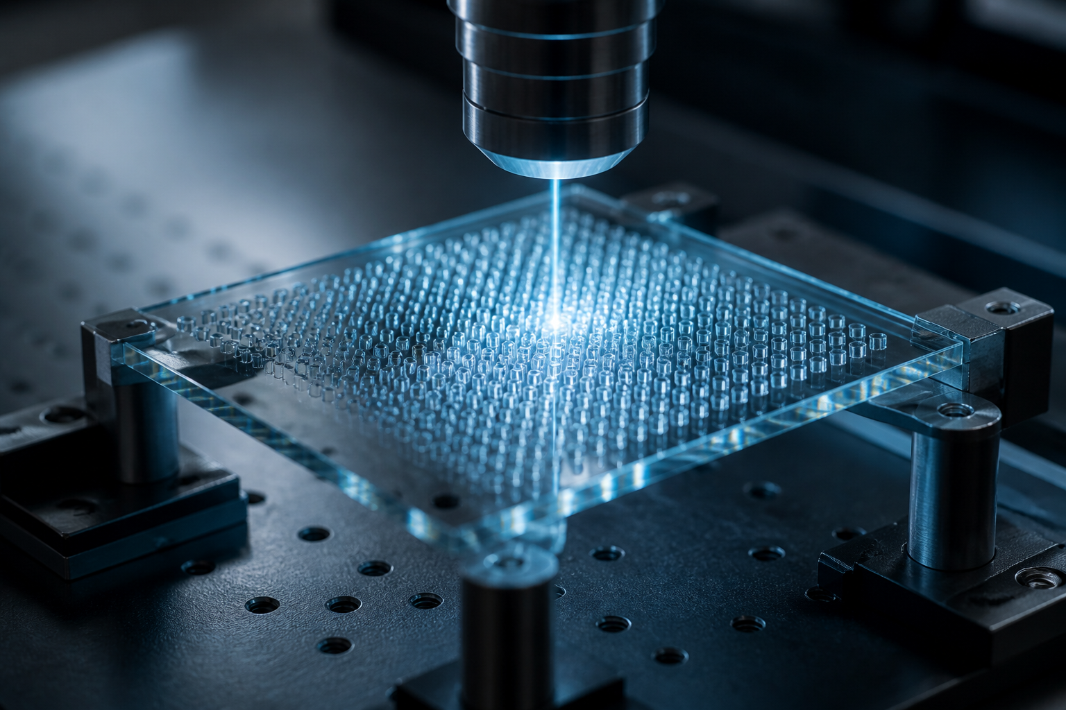
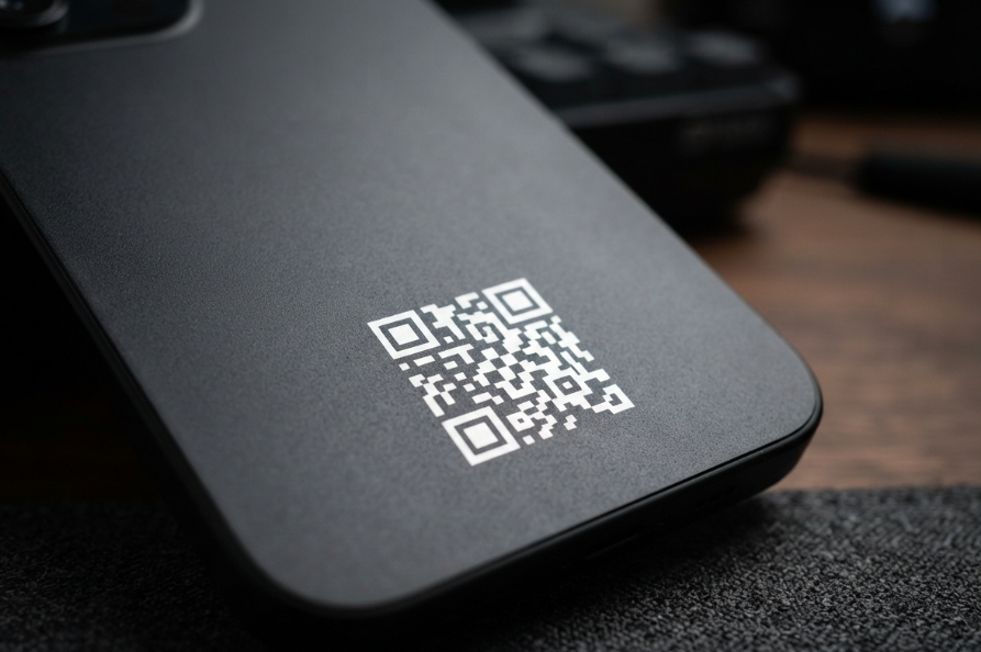
When manufacturing consumer electronics, the assumption is that “zero damage” means minimizing laser power. We see engineers constantly dialing back the power on their nanosecond fiber sources, terrified of burning delicate anodized housings. The result? Grey, low-contrast marks that fail automated vision-system reads 4% of the time, bottlenecking the entire assembly line. The physics of laser marking, however, dictates a counterintuitive approach. To achieve true zero-damage marking, you don’t go easy on the part—you outrun the heat.
“The prevailing assumption on the line was that ‘zero damage’ means minimizing power. So we dialed back the nanosecond fiber source, only to get low-contrast grey marks that failed vision-system reads 4% of the time. The physics flipped when we switched to a 10ps picosecond source: because pulse duration dropped below the electron-phonon coupling time (approx. 10ps), heat didn’t diffuse into the anodized layer. We actually increased peak power density, achieving a HAZ of <5µm and a 40% contrast bump on dark alumina housings. Zero thermal damage wasn’t achieved by going easy on the part—it was achieved by outrunning the heat.”
— process engineer, consumer electronics anodized housing marking line
This isn’t an isolated incident. Across the electronics manufacturing spectrum, from smartphone casings to PCB traceability, the secret to high-contrast, zero-damage laser marking lies in understanding thermal dynamics, not just turning down the power dial.
To achieve high-contrast, zero-damage laser marking on consumer electronics, you must match the laser’s pulse duration to the material’s thermal diffusion rate—typically using picosecond pulses. This approach vaporizes material before heat can spread, ensuring a minimal Heat-Affected Zone (HAZ) while maximizing peak power density for sharp, machine-readable contrast.
If you are sourcing or qualifying laser systems for consumer electronics, you are caught between two relentless pressures: the demand for flawless aesthetic quality and the demand for high-volume throughput. A smudged or burnt logo on a flagship smartphone is unacceptable; a slow marking cycle time on a 600-parts-per-hour wearables line is unprofitable.
In our experience qualifying laser systems for EMS (Electronic Manufacturing Services) providers, the same issues arise repeatedly. Engineers default to standard nanosecond fiber lasers because they are familiar and cheap. But when the substrate changes from steel to dark anodized aluminum, or from black plastic to white polymer, the nanosecond pulse suddenly becomes a blunt instrument. The heat diffuses, the material burns or foams inconsistently, and yield rates plummet.
The question of how to achieve high-contrast, zero-damage laser marking on consumer electronics components is therefore not just about aesthetics; it is a direct determinant of your production line’s profitability. When 1.2% of housings are scrapped due to poor beam quality, or when vision systems fail to read low-contrast QR codes, your margins evaporate. To solve this, we need to move past spec sheet buzzwords and look at the underlying physics of laser-material interaction.
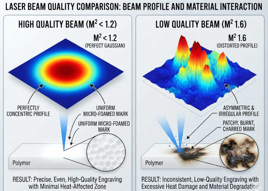
The foundation of zero-damage marking is confining the laser energy to the targeted area[1]. When a laser pulse hits a material, the energy is absorbed by electrons. These electrons then transfer their energy to the atomic lattice (phonons) as heat. This electron-phonon coupling time in metals and semiconductors is typically in the 1 to 10 picosecond range.
If your laser pulse is longer than this coupling time—such as a standard 10-nanosecond pulse—the heat has ample time to diffuse into the surrounding material. This thermal diffusion creates a Heat-Affected Zone (HAZ), leading to melting, recast, and discoloration. By switching to a picosecond (10ps) laser, the pulse duration is shorter than the time it takes for heat to spread. The material is removed through cold ablation before the heat can affect the surrounding area.
This is why the process engineer in our opening hook saw a 40% contrast bump on dark alumina housings. The picosecond pulse didn’t just reduce the heat; it bypassed the thermal diffusion phase entirely. When marking anodized aluminum, this precise control removes the anodization layer cleanly without melting the base aluminum beneath, resulting in a crisp, bright mark.
Common Mistake: Assuming lower power equates to lower damage. A low-power nanosecond laser will still heat the substrate slowly, often causing a larger, duller HAZ than a high-power picosecond laser.
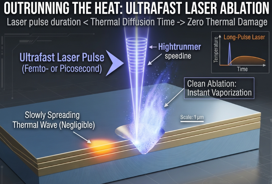
Once you have the correct pulse duration, the next variable controlling quality is the beam profile. This is defined by the M² (beam quality factor) value. A perfect Gaussian beam has an M² of 1.0. Many suppliers offer cheaper, higher-average-power lasers with an M² of 1.5 or 1.6.
Why does this matter for consumer electronics? Many white polymer casings rely on “micro-foaming”[2] for contrast. The laser locally heats the polymer, creating micro-bubbles that scatter light and appear white. If the M² value is poor, the focal spot has an uneven energy distribution—hot spots and cooler edges.
“For UV marking on white polymer casings, the spec sheets all push you toward higher average power to push throughput. But on a 6-month qualification for a wearables line, the deciding metric wasn’t power—it was M² and pulse stability. A 20W picosecond source with M²≤1.2 maintained <0.1% reject rate for micro-foaming contrast at 600 parts/hour. A higher-power, cheaper alternative with M² 1.6 caused inconsistent spot density, burning 1.2% of housings. The hidden cost of a poor beam parameter isn’t just the scrap; it’s the lost margin on a high-volume consumer contract.”
— R&D lead, EMS wearable device traceability marking
As this R&D lead observed, inconsistent spot density directly leads to scrap. A high M² value might seem like a minor spec sheet detail, but in a 600 parts/hour line, a 1.2% burn rate means 7.2 scrapped housings every hour. The raw average power means nothing if the energy distribution within the spot cannot reliably trigger uniform micro-foaming.
Light absorption varies drastically by material. Hitting a copper trace on a PCB with a 1064nm infrared laser will reflect most of the energy. Hitting a transparent glass cover with IR will pass right through. You must match the wavelength to the material’s absorption spectrum to ensure the energy is used for marking, not reflected or transmitted.
If you’re scaling up production, talking to a supplier directly can surface details no product listing will tell you.
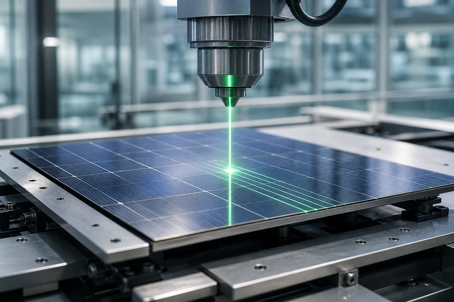
Even with the perfect laser, poor scanning destroys quality. The marking speed (how fast the galvo scanners move the beam) and the repetition rate must be synchronized to achieve the correct pulse overlap.
If the scan speed is too high relative to the rep rate, the pulses don’t overlap enough, resulting in a dashed, low-contrast line[3]. If the scan speed is too slow, too many pulses hit the same spot, leading to cumulative heat buildup and burning—the exact thermal damage you are trying to avoid.
Finding the “sweet spot” requires testing the hatch fill density, scan speed, and pulse overlap to find the parameters that yield the highest contrast just before the threshold of thermal damage.
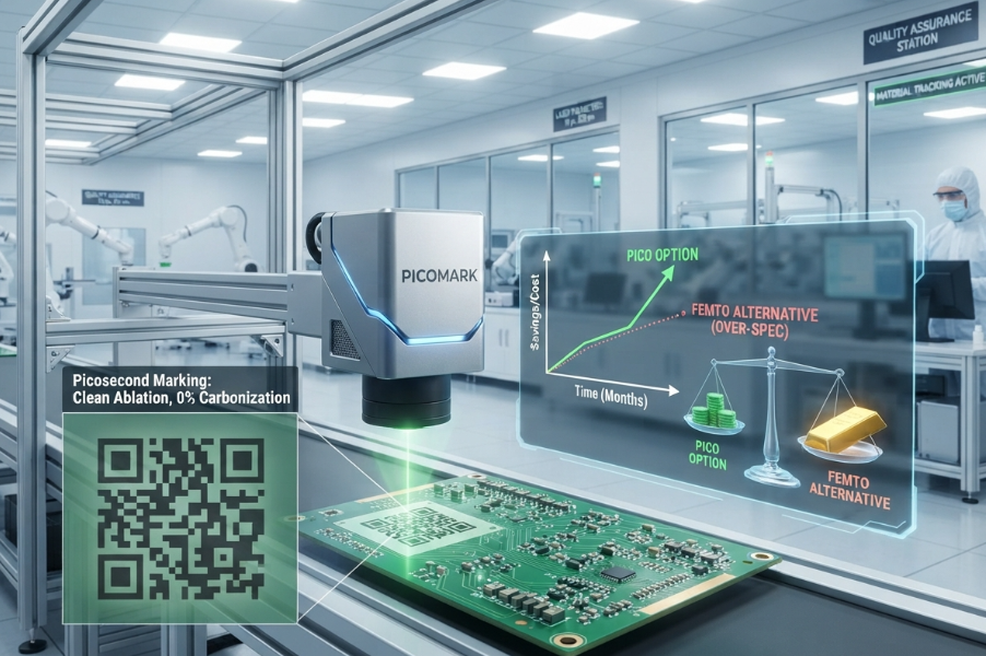
The final step in achieving the goal is financial: choosing the right tier of ultrafast laser. The default bias in the industry is to assume that the shortest pulse (femtosecond) and the highest power is the safest choice. But this often leads to severe spec redundancy, inflating your capital expenditure without adding value.
“When qualifying a light source for PCB QR-code marking, the default bias was toward femtosecond—shortest pulse, lowest risk of substrate delamination, the safe call. Then the ROI calculation hit. The 2D codes required ±15µm resolution and zero char on FR4, which a 50W picosecond source achieved at 3.2x the marking speed of the fs alternative. The fs source protected a thermal tolerance the FR4 substrate never actually required. We integrated the ps laser, held zero-damage specs, and cut the system payback period from 26 to 14 months.”
— laser system integrator, PCB traceability marking equipment selection
For FR4 PCBs, the material’s thermal tolerance does not require sub-1ps pulse durations. A 10ps picosecond pulse is already fast enough to prevent carbonization (charring). Choosing a femtosecond laser for this application means you are paying a 40-50% premium for thermal protection you don’t need. Worse, femtosecond lasers often have lower average power or require massive speed reductions to maintain pulse energy, dropping your throughput by up to 3x. The smartest decision is finding the longest pulse duration that still achieves zero-damage, maximizing both speed and ROI.
To specify the right system for your line, use this framework:
Choosing a laser marking system requires balancing physics, material science, and economics. Data sheets won’t tell you how a laser interacts with your specific polymer blend or anodization thickness. You need empirical data. If you’re sourcing at scale, talking to a supplier directly can surface details no product listing will tell you.
The pursuit of zero-damage marking often leads engineers down the wrong path of lowering power and hoping for the best. But as the physics shows, quality is not achieved by being gentle; it is achieved by being fast. Outrunning the heat, controlling the beam profile, and matching the technology to the actual material tolerance are what separate a profitable line from a scrap-generating one. In consumer electronics marking, you don’t win by turning down the power; you win by mastering the time.
Why does nanosecond laser marking cause heat damage on electronics?
Nanosecond laser pulses (typically 1-100ns) last longer than the electron-phonon coupling time in metals (1-10ps). This means the laser energy has time to convert into heat and diffuse into the surrounding material, creating a Heat-Affected Zone (HAZ) that causes melting, warping, or discoloration on sensitive components.
Is picosecond or femtosecond better for consumer electronics marking?
For most consumer electronics applications (like anodized aluminum, plastics, and PCBs), picosecond lasers (approx. 10ps) offer the best balance of quality and cost. They are fast enough to prevent heat damage (cold ablation) while offering higher throughput and lower capital costs than femtosecond lasers, which are often unnecessarily expensive “spec redundancy.”
What is the best laser for white plastic casings?
For white polymer casings, a picosecond UV (355nm) or green (532nm) laser is typically best. This allows for “micro-foaming,” where the laser locally creates micro-bubbles that scatter light for a high-contrast white mark. The success of this process relies heavily on excellent beam quality (M² ≤ 1.2) to ensure uniform foaming.
How does laser M² affect marking yield?
M² (beam quality factor) determines the energy distribution in the focal spot. A poor M² (>1.5) means an uneven spot with hot spots and cooler edges. This causes inconsistent marking, leading to burning in some areas and low contrast in others, which spikes the reject rate on high-volume lines.
Can laser marking damage the internal components of a smartphone?
No, not if specified correctly. Ultrafast picosecond lasers confine their energy to the surface layer (e.g., the anodization) through cold ablation. Because the pulse duration is shorter than the thermal diffusion time, no heat reaches the sensitive internal electronics or battery beneath the housing.
What is the ROI of upgrading to an ultrafast laser for electronics?
Upgrading from a nanosecond to a picosecond laser usually increases capital expenditure, but the ROI is driven by yield improvements. By dropping reject rates from 4% to under 0.1%, and avoiding secondary cleaning operations, most high-volume consumer electronics lines see a system payback period of 12 to 18 months.
[1]”Thermal Limitations in Ultrafast Laser Direct Writings in … – PMC”. Ultrafast laser-material interaction studies describe how shortening the pulse duration can limit thermal diffusion and localize deposited energy, which provides the physical basis for reduced heat-affected zones in precision laser processing. Evidence role: mechanism; source type: paper. Supports: The foundation of zero-damage marking is confining the laser energy to the targeted area.. Scope note: This supports the general mechanism of spatial and thermal confinement; it does not by itself prove that any specific marking process causes zero damage.→
[2]”Laser-Induced Microstructuring of Polymers in Gaseous … – PMC”. Laser marking literature describes foaming in polymers as a mechanism in which localized laser heating generates gas-filled microvoids or bubbles that increase diffuse light scattering and produce a lighter, often white, mark. Evidence role: mechanism; source type: paper. Supports: White polymer casings can use laser-induced micro-foaming to create high-contrast white marks.. Scope note: This supports the general marking mechanism in polymers; it does not by itself establish how widely the method is used across all consumer electronics casings.→
[3]”Effect of Laser Pulse Overlap and Scanning Line … – PMC”. Laser micromachining and marking literature describes pulse-to-pulse spacing as a function of scan speed and repetition rate, and notes that insufficient spatial overlap can produce discontinuous or weakly formed tracks. Evidence role: mechanism; source type: paper. Supports: When scan speed is too high relative to repetition rate, pulse overlap is insufficient and the marked line can become discontinuous or low contrast.. Scope note: This supports the mechanism generally; the exact threshold for a dashed or low-contrast line depends on material, optics, pulse energy, and process settings.→