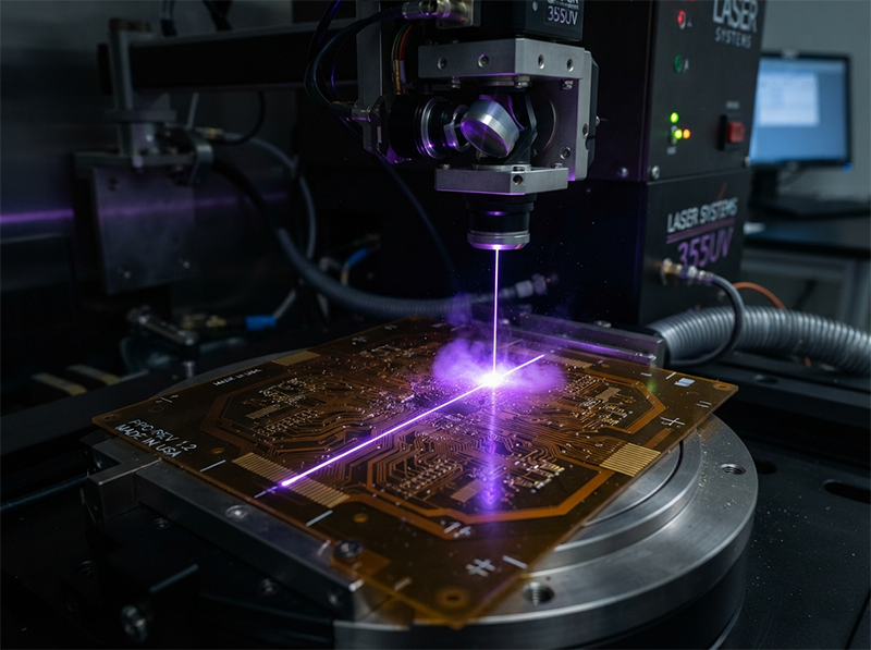
Every process engineer knows the feeling. The line is running at 95% yield, hitting all its targets. Then a new batch of coverlay film arrives, or the ambient humidity shifts two degrees, and suddenly the “sweet spot” for your nanosecond laser process vanishes. What was a clean cut is now a mess of carbonized edges and melted adhesive. You spend the next shift tweaking power, frequency, and scan speed, chasing a narrow process window that seems to move on its own.
This daily battle isn’t a sign of a bad engineer; it’s the signature of a fundamentally limited tool. The standard industry view is that picosecond lasers are better simply because they are “colder.” This is true, but it misses the entire point.
The real value of a 355nm UV picosecond laser, especially in complex multi-layer materials like FPC or LCP, isn’t just achieving lab-grade “zero heat damage.” It’s about fundamentally widening the process window. It transforms a process where “not burning the material” is a constant variable you must control, into a physical default state. This allows engineers to aggressively pursue throughput without fearing the catastrophic yield loss that is always one parameter drift away with older laser technologies.
This insight changes the conversation from a lab discussion about heat-affected zones (HAZ) to a factory floor discussion about yield, uptime, and cost per part. It explains why leading manufacturers are adopting this technology not just for precision, but for predictability at scale.
355nm UV picosecond lasers excel at fine processing not just by minimizing heat, but by fundamentally decoupling the physical properties of multi-layer materials like flexible printed circuits (FPC) and liquid crystal polymer (LCP). This transforms an unstable, variable-sensitive task into a stable, highly repeatable manufacturing operation. The result is a dramatically wider process window, higher Overall Equipment Effectiveness (OEE), and the unique capability to mass-produce next-generation electronic components.
The components inside our devices—from smartphones to automotive sensors—are becoming smaller, more complex, and built from advanced composite materials. A modern 5G antenna module may involve cutting through a stack of copper (Cu), liquid crystal polymer (LCP), and polyimide (PI), each with wildly different thermal and optical properties.
For years, nanosecond UV lasers were the workhorse for these tasks. But as tolerances tighten and material stacks become more challenging, their fundamental limitation becomes a critical business problem. Nanosecond pulses are long enough for significant heat to diffuse from the laser spot, especially along conductive layers like copper. This leads to delamination, melted adhesive, and a process that is exquisitely sensitive to the slightest variation in material batch or environmental conditions.
Engineers are therefore spending less time innovating and more time firefighting—constantly re-qualifying processes to chase a narrow, shifting “sweet spot.” This article breaks down why the shift to 355nm picosecond technology is not an incremental improvement, but a necessary step-change that addresses the core physics of the problem and unlocks significant commercial value in three distinct layers: process stability, production efficiency, and future market access.
The most common selling point for picosecond lasers is “cold ablation.” Because the pulse duration (around 10 picoseconds) is shorter than the time it takes for thermal energy to diffuse into the surrounding material, the heat-affected zone is virtually nonexistent. This is correct, but it’s a lab-level benefit. The factory-level benefit is far more significant.
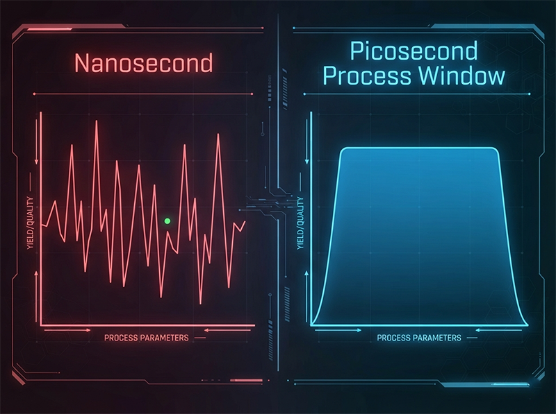
With a nanosecond laser cutting FPC coverlay, the energy delivered is a delicate balance. Too little, and the cut is incomplete. Too much, and the underlying PI film carbonizes or the adhesive melts, creating a “yellow ring” defect. The window for success is a tightrope.
A 355nm picosecond laser changes the physics entirely. The material is ablated—essentially vaporized—before it has a chance to conduct heat. “Not burning” is no longer a parameter to be carefully balanced; it becomes the default state of the process.
This is what we mean by a radically wider process window.
1.Before (Nanosecond Laser): The process engineer defines a narrow power and speed range that works for a specific batch of material. Any drift in laser output, material thickness, or even ambient temperatur1e can push the process out of this window, causing yield to crash. Throughput is intentionally limited to stay safely within the narrow window.
2.After (Picosecond Laser): The “no burn” floor is so robust that the engineer can now focus almost exclusively on the ceiling: maximizing speed and power to increase throughput. The process becomes resilient to material and environmental variations. What was once a variable to be controlled becomes a constant you can rely on.
This shift moves the engineer’s job from a reactive, problem-solving role to a proactive, optimization-focused one.
The second-order effect of “cold ablation” is a cleaner process. Nanosecond ablation often creates a hot plasma plume and molten ejecta that can redeposit on the workpiece and, more critically, on the laser’s own optics. Picosecond ablation produces a finer, “drier” vapor and nanoparticle debris.
Again, the benefit is not just a cleaner part. It’s a direct, quantifiable impact on Overall Equipment Effectiveness (OEE), a key metric for any production manager.
The hot, sticky debris from nanosecond lasers coats the protective windows, scanning galvanometer mirrors, and f-theta lenses in the beam path. This contamination has two major consequences:
1.Power Density Drop-off: The coated optics absorb and scatter laser energy, reducing the power density at the work surface. A process qualified at the start of a shift may fail by the end of the shift, not because the laser’s output changed, but because the beam delivery system is compromised.
2.Increased Unplanned Downtime: To combat this, production lines must schedule frequent stops for optical cleaning and system recalibration. This “hidden downtime” is a major drain on OEE and is rarely factored into the theoretical cost-per-part calculation.
Based on our experience with customers transitioning from nanosecond to picosecond UV systems for high-volume FPC cutting, the impact on uptime is dramatic. We have seen lines move from a typical OEE availability of 85-90% to a sustained 98% or higher. The cost of a few hours of unplanned downtime per week often exceeds the initial cost delta between the laser systems within the first year.
| Metric | Nanosecond UV Laser Process | 355nm Picosecond UV Laser Process | Impact on OEE |
|---|---|---|---|
| Debris Type | Molten ejecta, hot plasma | Fine, “dry” nanoparticles | Reduced optical contamination |
| Optics Cleaning Cycle | Every 4-8 hours of operation | Every 24-48 hours or longer | Significant increase in Uptime |
| Process Stability | Drifts as optics get dirty | Highly stable over long runs | Improved Quality Rate |
| Effective Throughput | Limited by cleaning downtime | True throughput matches spec | Higher Performance Rate |
If your line requires frequent stops for optics cleaning, investing in a picosecond source can deliver a more significant return through OEE improvement than by simply increasing theoretical processing speed.

The final layer of value is strategic. The ability of 355nm UV picosecond lasers to process a wide range of materials is often framed as a benefit of versatility. The real value is that it provides the only viable mass-production pathway for certain next-generation products.
Consider a 5G antenna module with a Cu/LCP/Cu stack. Liquid Crystal Polymer (LCP) is a fantastic dielectric for high-frequency signals, but it’s notoriously difficult to process in a composite stack.
This capability is not a “nice-to-have.” For a component manufacturer, it is the admission ticket to the 5G, high-frequency communications, and automotive radar supply chains. Choosing a 355nm picosecond UV laser is not just an equipment upgrade; it’s a strategic decision that enables the business to compete for high-value contracts that are physically impossible to fulfill with older technology.

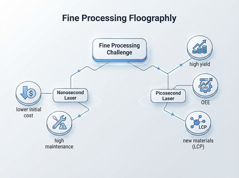
When deciding on a laser source for fine processing, the choice is clearer when framed by business outcomes, not just technical specs:
The true performance of a laser is not revealed on a datasheet, but on a production line running for 24 hours. The stability of the pulse, the quality of the beam, and the resilience of the optical system to the process environment are what determine your final cost per part. A laser that looks good in a 10-minute demo might fail to hold its process window over a full shift.
Before committing to a production ramp, it’s critical to verify these performance characteristics under real-world conditions.
If you’re sourcing at scale, talking to a supplier directly can surface details no product listing will tell you.
We began with the process engineer’s struggle to find a stable “sweet spot.” The fundamental shift offered by 355nm UV picosecond technology is that it doesn’t just help you find the sweet spot—it expands that spot into a vast, forgiving plateau. It decouples the complex material physics from the manufacturing process, making the outcome predictable and repeatable.
This changes the entire economic equation of fine processing. It moves the focus from mitigating defects to maximizing throughput.
The value of a 355nm UV picosecond laser isn’t just in the precision of the cut; it’s in the predictability of the entire manufacturing process it unlocks.
[1] Du, K., et al. (2018). High-Quality Cutting of Flexible Printed Circuits by a Picosecond Laser. Lasers in Manufacturing and Materials Processing, 5(4), 419-432.
🔗 https://doi.org/10.1007/s40516-018-0071-8
[2] Neuenschwander, B., et al. (2014). Processing of metals and brittle materials with ps-laser pulses: A review. Journal of Laser Applications, 26(4), 042009.
🔗 https://doi.org/10.2351/1.4891289
[3] An, R., et al. (2017). A comparative study on debris and recast layer of nanosecond and picosecond laser milling of a nickel-based single crystal alloy. The International Journal of Advanced Manufacturing Technology, 93(5-8), 2605-2616.
🔗 https://doi.org/10.1007/s00170-017-0749-9
[4] Zheng, H. Y., et al. (2020). Laser drilling of through glass vias (TGVs) for 3D integration. Journal of Physics: Photonics, 2(2), 022003.
🔗 https://doi.org/10.1088/2515-7647/ab71c0
[5] Ihlemann, J., et al. (1992). Ablation of polymers with picosecond and nanosecond UV laser pulses. Applied Surface Science, 54, 193-198.
🔗 https://doi.org/10.1016/0169-4332(92)90317-H