Within the family of picosecond ultrafast lasers, infrared picosecond lasers are highly versatile; green‑light picosecond lasers have made deep inroads into the photovoltaic sector; and ultraviolet picosecond lasers (355 nm), thanks to their shorter wavelengths and higher photon energy, have become the preferred light source for micro‑ and nano‑scale precision processing. This article examines waveband principles, product performance, and typical applications across three dimensions to help you understand the core strengths of ultraviolet picosecond technology.
A picosecond laser uses extremely short pulses—on the order of one trillionth of a second—to suppress heat diffusion and achieve a cold‑processing effect.Different picosecond lasers are suited to specific applications. The 355nm ultraviolet laser holds unique advantages in micro-nano precision processing: On one hand, when the focusing optical conditions remain consistent, the laser wavelength determines the minimum spot size limit. Since ultraviolet light has a shorter wavelength, it can achieve smaller focused spots, enabling sub-micron-level processing. On the other hand, photon energy is inversely proportional to wavelength: the shorter the wavelength, the more energy each individual photon carries. The energy of ultraviolet photons can directly break chemical bonds between a material‘s molecules, resulting in an extremely small heat‑affected zone and virtually eliminating problems such as thermal deformation, burrs, or chipped edges—thus ensuring high‑quality processing of fine structures.
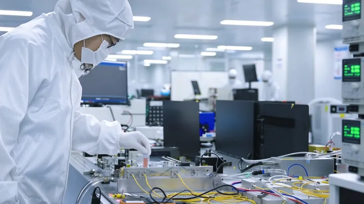
△ Ultrafast Solid Laser Processing Site
The theoretical advantages of a given band must ultimately be realized in industrial mass‑production scenarios。Huachuang Hongdu’s ultraviolet picosecond laser relies on its own proprietary solid‑state laser amplification technology to convert its fine‑processing capabilities in the ultraviolet spectrum into stable, reliable mass‑production capacity, thereby creating three core product advantages.
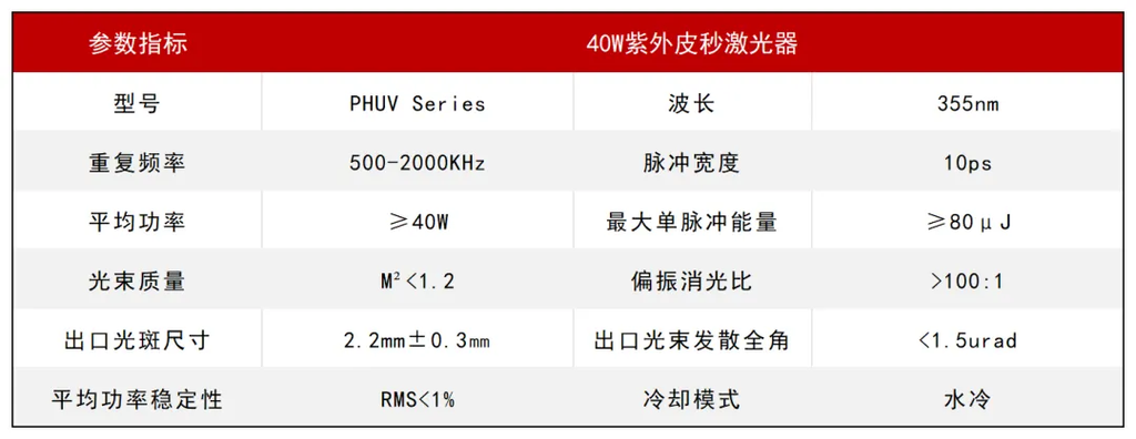
△ Technical Parameters of 40W UV Picosecond Laser (Can be Customized on Demand)
① Short wavelength fine processing, clean edges without carbonization
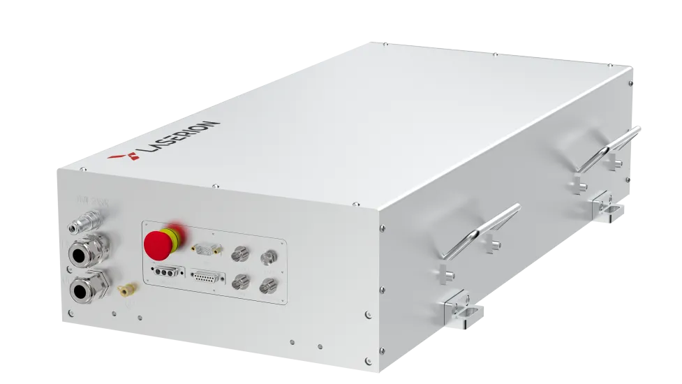
△ Huachuang Hongdu Ultraviolet Picosecond Laser
The 355nm band can obtain a smaller focusing spot for sub-micron processing. The material is directly stripped, and the side wall of the incision is clean, usually free of melting, carbonization, and residues; When processing flexible substrates and thin media films, we can avoid blacking and layered drumming, and meet the strict appearance and reliability requirements of high-end electronic components.
② Excellent beam quality, high process consistency
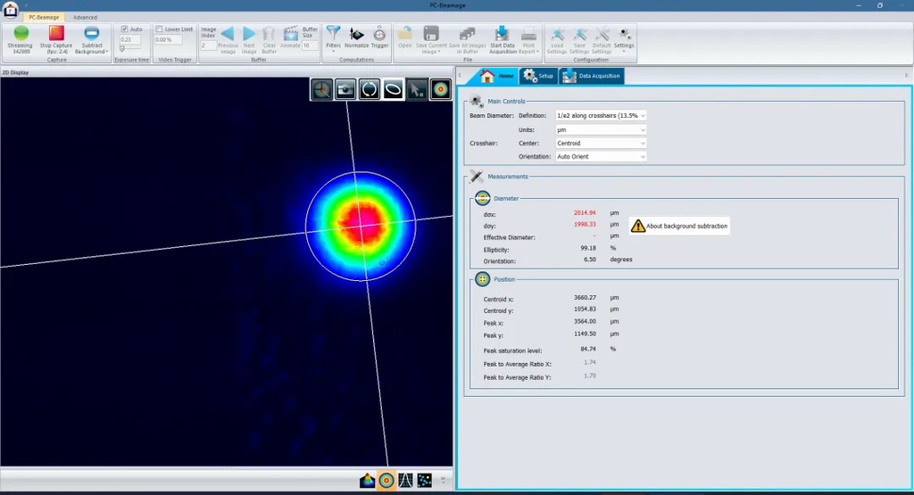
△ Typical Photospots of Ultraviolet Picosecond
A ultraviolet picosecond laser M²< 1.2 ,The energy concentration is high. When working with large area array micropores and continuous line grooves, the light spot energy is distributed evenly, the pore type is correct, and the side wall is vertical.When used in conjunction with a high‑speed scanning mirror system, processing consistency is excellent , ensuring stable yield rates for mass‑produced products.
③ Power is stable and reliable, suitable for long continuous production
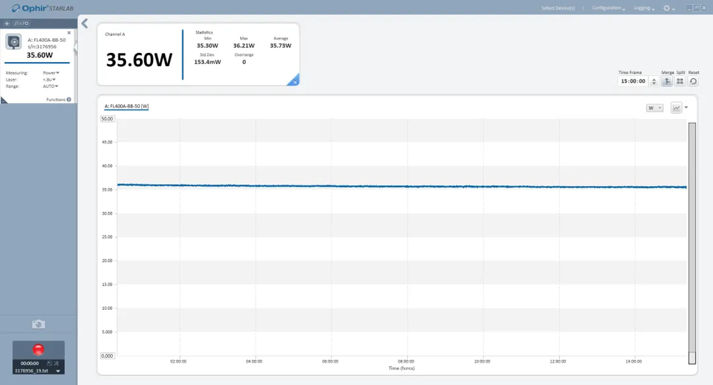
△UV Picosecond RMS Power Stability Test Results
The entire device incorporates a self‑developed cavity and an ultraviolet‑resistant optical design to reduce ultraviolet damage to components。Customized temperature control heat dissipation ensures power stability under high load.The fully digital, closed‑loop electronic control system monitors crystal temperature and pump current in real time; single‑pulse energy fluctuations are minimal, and the system supports continuous production for 24 hours.The modular design makes maintenance easy, facilitates integration with automated production lines .
Relying on its “ultra‑precise, low thermal loss, and non‑carbonizing” core characteristics, ultraviolet picosecond technology continues to solve key challenges in microfabrication processes within the microelectronics field. We have already discussed, in detail in our previous process case studies, the practical aspects of cutting thin metal materials and the key challenges associated with the process. This article will focus on practical applications in areas related to semiconductors.
Application 1: FPC cutting of flexible electric circuit board
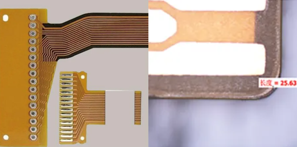
△ FPC Cutting
FPC is widely used in the mobile device sector because of its light weight and flexibility. Ultraviolet skin second uses non-contact high-precision contour processing, without scratches, fast processing speed, effectively shortening the production cadence, and suitable for a variety of materials and laminate structures.After processing, there is no need to perform carbon‑removal cleaning; this simplifies the process and improves the production yield of high‑density FPCs.
Application 2: PCB / carrier board precision micro-machining
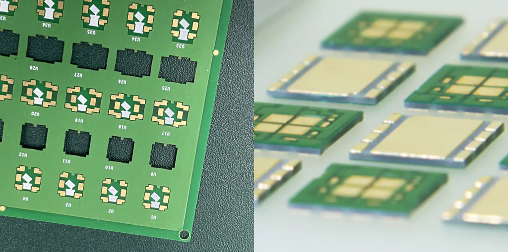
△ PCB Flash Machining
Ultraviolet picosecond technology can be used to precisely cut single‑layer and multi‑layer PCBs, replacing conventional milling processes; it produces clean edges without burrs and generates little dust, making it ideal for areas with high‑density component wiring。For semiconductor packaging substrates and high‑end PCBs, ultraviolet picosecond technology can selectively remove target film layers from dielectric films, solder‑mask openings, and micro‑grooves; this causes minimal damage to underlying copper traces, produces sharp edge profiles, and meets the requirements of high‑density interconnection processes.
Application 3: Pre-formed welding cutting
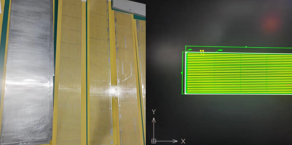
△ Pre-formed Welding Cutting
Pre‑formed solder sheets are precision brazing materials used for semiconductor power devices and optical chip packaging. The ultraviolet skin second sewing is fine and controllable, which can achieve narrow sewing machining and greatly improve the material utilization rate.Non‑contact processing eliminates burrs, curled edges, and hardening problems; when combined with small‑area, segmented processing, it produces weld‑sheet products with excellent flatness and can easily process complex, irregular shapes such as L‑shaped pieces, pieces with notches, and fine grid lines—making it highly adaptable to customized packaging requirements.
Micron manufacturing continues to iterate toward smaller size and higher cleanliness, and processing no longer only seeks to “cut to move,” but to “cut fine, cut clean, and batch stable.” Huachuang Hongdu ultraviolet picosecond lasers are used to stabilize industrial-grade light sources and help customers overcome bottlenecks in micro-nano manufacturing.