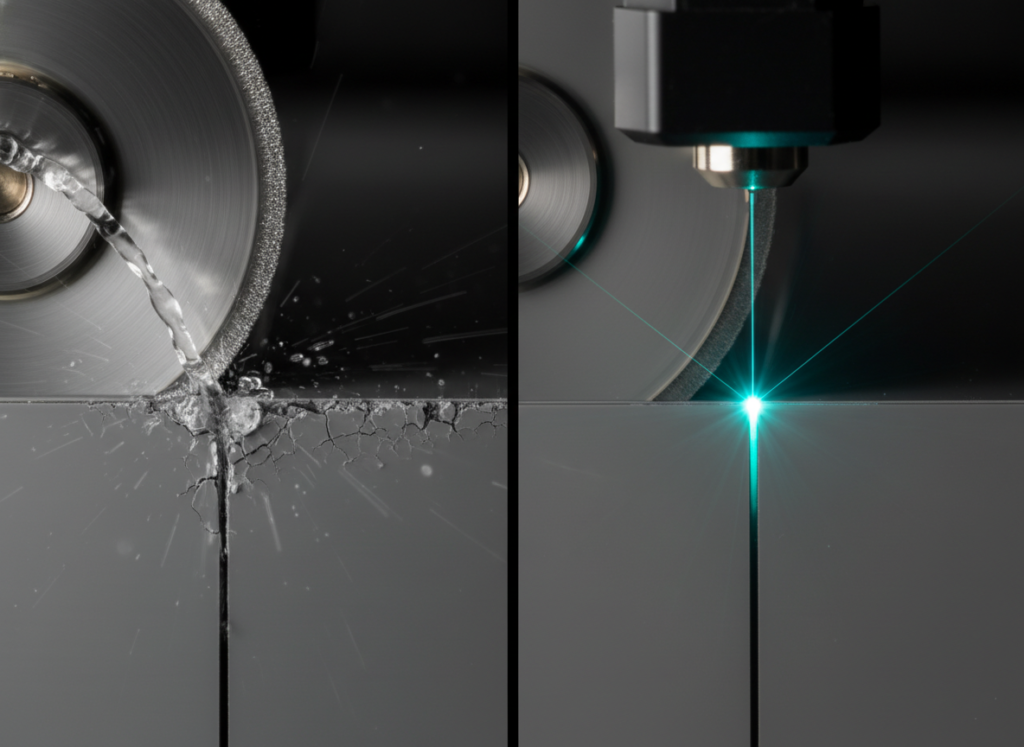
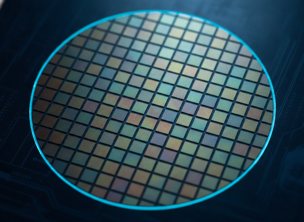
For decades, separating dies from a wafer meant one thing: a spinning diamond blade. It still works for plenty of wafers. The reason ultrafast lasers keep taking over the hard cases is not that the blade got worse — it is that wafers changed faster than the blade could follow.
“We stayed with blade dicing because it was qualified and fast, and on thick wafers it was fine. Then the product moved to a thinner, low-k wafer and the blade started tearing it — delamination along the street, chipping we couldn’t dial out at any feed rate. It wasn’t a tuning problem; the mechanical contact was the problem. Ultrafast laser scribing removed the contact and the chipping with it, and the thin wafer survived. The blade hadn’t gotten worse — the wafer had moved past what a blade can do.” — process engineer, wafer dicing line
I take that account seriously because it reframes the whole question. Ultrafast laser wafer dicing is not simply a faster blade. It removes material by a different physical mechanism, and that difference is what lets it handle the thin, brittle, and low-k wafers where mechanical contact fails. To see why, it helps to separate two processes people often blur together.
Ultrafast laser wafer dicing removes material with ultrashort pulses that vaporize it before heat spreads, producing a narrow kerf with minimal chipping and a small heat-affected zone. Dicing cuts fully through the wafer; scribing cuts a shallow groove so the wafer can be cleaved along it. Because there is no mechanical contact, the laser avoids the chipping, cracking, and delamination a blade causes on thin or low-k wafers — which raises die break strength and yield.
Singulation sits at the end of the wafer’s value chain, after every expensive process step has already been paid for. Damage a die here and you scrap the most valuable version of it. That is what makes the dicing method a yield decision, not a finishing detail.
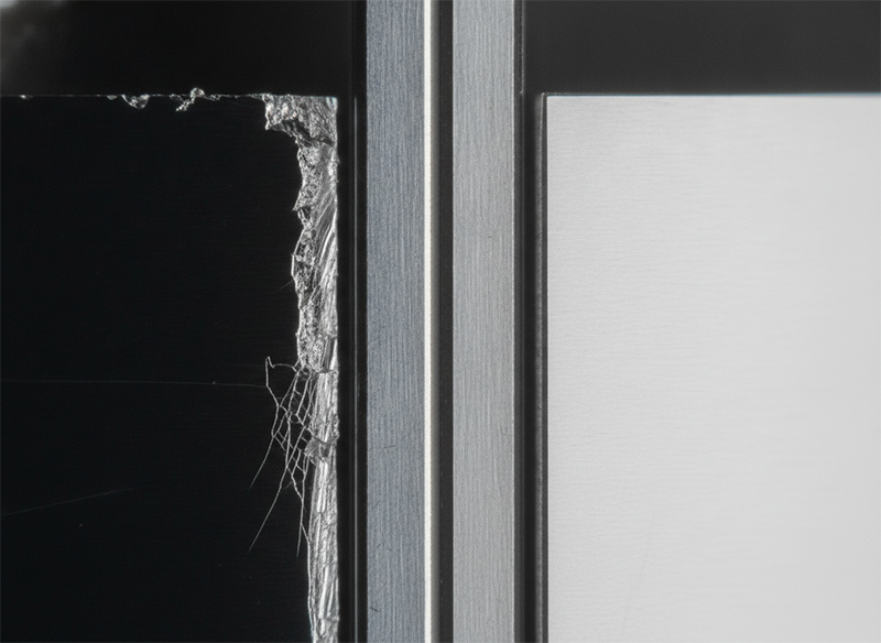
The pressure is structural. Wafers keep getting thinner, dies keep getting smaller, and low-k dielectrics and compound semiconductors keep getting more fragile. Below roughly 100 µm of thickness, blade dicing tends to cause chipping, cracks, delamination, and residual stress that drop yield sharply. The blade did not change — the wafers moved into territory where mechanical contact is the liability.
Across wafer singulation work, the teams that hold yield on advanced wafers treat ultrafast laser wafer dicing as the enabling process, not a luxury. The sections below separate dicing from scribing, explain how the laser actually removes material, and show why die break strength — not how clean the street looks — is the number that decides whether the process is working.
The two terms get used loosely, but they describe different cuts. Dicing means cutting fully through the wafer to separate the dies in one operation. Scribing means cutting only a shallow groove along the street, then breaking or cleaving the wafer along that weakened line in a separate step.
The choice is a trade. Full laser dicing is a single operation and works regardless of crystal orientation, which matters for non-silicon materials. Laser scribing followed by a controlled break can be faster on some wafers and leaves less material to ablate, but the cleave quality depends on the groove and the material. For brittle compound semiconductors and patterned wafers, the right answer depends on die size, thickness, and what the downstream package needs from the edge.
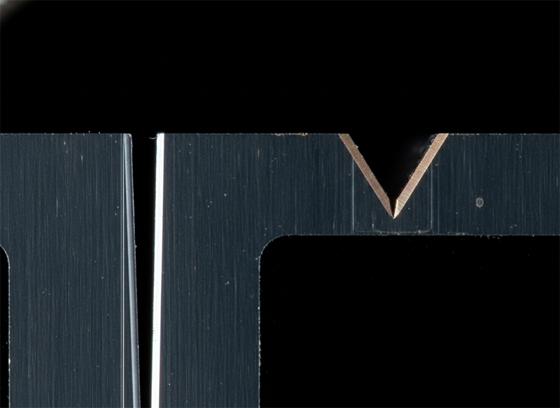
The mechanism is what sets ultrafast dicing apart from both the blade and longer-pulse lasers. An ultrashort pulse deposits its energy and vaporizes material faster than heat can diffuse into the surrounding silicon, so the material leaves as vapor or plasma and carries the energy with it. This near-cold ablation is why the cut comes out with a small heat-affected zone instead of a melted, stressed rim.
Two consequences follow directly. The kerf is narrow, because the beam can be focused tightly and there is no physical blade width to accommodate. And the edge is clean, because there is no mechanical force prying at a brittle material and no wide thermal zone seeding cracks. On thin wafers, laser ablation produces smaller chipping on both the top and bottom of the die and a narrower kerf than a blade, which is exactly what fragile, small-die products need.
Here is the measurement that separates a process that looks good from one that lasts.
“I used to judge a dicing process by how clean the street looked. The metric that actually predicted field returns was die break strength. A blade leaves micro-cracks along the diced edge that pass visual inspection and then propagate under thermal cycling in the field. Ultrafast laser dicing, with its minimal heat-affected zone, left edges that held far higher break strength on the same wafer. The defect that mattered wasn’t on the surface I was inspecting — it was in the edge I wasn’t testing.” — reliability engineer, die-level qualification
Die break strength measures how much stress a singulated die can take before it fractures, and it is governed by the micro-cracks along the diced edge. A blade leaves edge damage that can pass a visual check and then grow under thermal cycling in the field, surfacing as a die crack long after the wafer left the fab. Because ultrafast laser dicing keeps the heat-affected zone small and avoids mechanical edge damage, it has been shown to improve front- and backside breaking strength compared to mechanical dicing. The defect that drives field returns lives in the edge, not on the surface — which is why break strength, not appearance, is the number to qualify against.
| Dimension | Blade Dicing | Ultrafast Laser Dicing |
|---|---|---|
| Contact | Mechanical (physical blade) | None (optical) |
| Kerf width | Wider (blade thickness) | Narrow |
| Chipping | More, top and bottom | Less, both sides |
| Thin / low-k wafers | Chipping, cracks, delamination below ~100µm | Handles cleanly |
| Die break strength | Lower (edge micro-cracks) | Higher (minimal HAZ) |
| Speed (example, full sawing) | ~25 min | ~3–5 min |
| Best fit | Thick, robust wafers | Thin, brittle, low-k, compound semis |
The table shows why the switch happens at the hard end of the spectrum: the wafers that break blades are the ones lasers handle best.
“The blade process looked cheaper per wafer until we counted dies per wafer. A wider blade kerf eats street width, and on a small-die product that lost real estate adds up to fewer dies on every wafer. Switching to a narrow ultrafast laser kerf recovered street width we’d been throwing away — more dies per wafer, plus fewer edge-chip rejects. The laser wasn’t faster per cut on every job, but it was more dies per wafer, and that’s the number that pays for the tool.” — manufacturing engineer, high-volume die production
The economics of dicing live in two numbers: how many dies fit on a wafer, and how many survive singulation. A narrow kerf widens the first by reclaiming street width a wide blade consumes, which matters most on small-die products where street area is a real fraction of the wafer. Lower chipping widens the second by cutting edge-chip rejects. Cost per good die — not cost per wafer — is the figure that reaches the bottom line, and on advanced wafers it usually favors the laser.
If your wafers are thin, low-k, or compound semiconductor, and blade dicing is fighting you with chipping or delamination, move to ultrafast laser wafer dicing — for those materials it is enabling, not just better. If your priority is die break strength and field reliability, qualify on break strength and the laser’s small heat-affected zone earns its place. Choose scribing when a groove-and-break suits your material and die geometry, and full dicing when you need a single through-cut independent of crystal orientation.
If your wafers are thick and robust and your dies are large, blade dicing may still be the economical choice — the laser’s advantages concentrate where wafers are fragile and street area is precious. Match the method to the wafer, not to the equipment you already own.
A few variables decide more than the cut type: your wafer thickness and material, your die size and the street width you can afford, and whether your reliability spec is driven by die break strength. Each one shifts where the laser pulls ahead of the blade.
Those details are hard to settle from a datasheet. If you are qualifying a singulation process at scale, talking to an application engineer who has diced your wafer type can surface trade-offs no product listing will tell you.
The team that switched did not abandon a working process — they followed the wafer to where the blade could no longer go. That is the quiet truth of ultrafast laser wafer dicing: it wins not by being a faster blade, but by removing the mechanical contact that fragile wafers cannot survive. As wafers keep getting thinner, the question stops being whether to move to laser dicing and becomes when. The edge you cannot see is the one that decides yield.
What is the difference between wafer dicing and scribing? Dicing cuts fully through the wafer to separate the dies in one operation. Scribing cuts only a shallow groove along the street, after which the wafer is broken or cleaved along that line in a separate step. Dicing works regardless of crystal orientation; scribing leaves less material to ablate but depends on cleave quality.
How does ultrafast laser wafer dicing work? An ultrashort pulse vaporizes material before heat spreads into the surrounding silicon, so the ablated material carries the energy away. This near-cold ablation produces a narrow kerf with minimal chipping and a small heat-affected zone, without the mechanical contact that causes blade chipping on thin or brittle wafers.
Is laser dicing better than blade dicing? For thin, low-k, and compound-semiconductor wafers, yes. Laser dicing produces less chipping, a narrower kerf, and higher die break strength, and it handles wafers below about 100 µm where blades cause cracks and delamination. For thick, robust wafers with large dies, blade dicing can still be economical.
Does laser dicing increase die strength? It can. Ultrafast laser dicing keeps the heat-affected zone small and avoids the mechanical edge damage a blade leaves, which has been shown to improve front- and backside die breaking strength. Higher break strength means fewer die cracks under thermal cycling in the field.
Can you dice thin wafers with a laser? Yes, and it is one of the main reasons to use a laser. Below roughly 100 µm, blade dicing tends to cause chipping, cracks, delamination, and residual stress. Ultrafast laser dicing removes material without mechanical contact, letting thin wafers singulate cleanly with higher yield.
What is the kerf width of laser dicing? Laser dicing produces a narrower kerf than a blade because the beam focuses tightly and there is no physical blade width. The narrower kerf reclaims street width, which can increase the number of dies per wafer — a meaningful gain on small-die products.
Is laser dicing faster than blade dicing? Often, yes. In one comparison, laser ablation completed wafer sawing in 3 to 5 minutes versus about 25 minutes for blade dicing. Speed depends on wafer thickness and material, but the larger advantage is usually fewer rejects and more good dies per wafer, not raw cut time alone.
Which wafers need ultrafast laser dicing? Thin wafers, low-k dielectric wafers, compound semiconductors, and small-die products benefit most. These are the cases where blade contact causes chipping or delamination and where die break strength and street area drive yield. For thick, robust silicon with large dies, blade dicing may remain sufficient.