Most teams frame this as a ranking question — which mode is more sensitive, which one to standardize on. That framing is where inspection coverage quietly springs a leak. Bright-field and dark-field do not sit on a quality ladder. They see different defects, and choosing one over the other decides what you can detect at all.
“We built the line around bright-field because it gave us the detailed pattern images everyone wanted to see. It ran clean for months — until a particle excursion walked straight through us to the customer. Bright-field wasn’t under-sensitive to those particles; it was nearly blind to them. The sub-micron particles scattered light at angles bright-field never collected. Adding a dark-field channel caught them on the first wafer. The mode you choose doesn’t just set sensitivity — it sets which defects you can see at all.” — process integrator, wafer inspection line
I take that account seriously because it reframes the whole decision. The question is not which mode wins. It is which defect class you are hunting, and whether your illumination can physically collect the signal that defect produces.
Use bright-field inspection for pattern defects on patterned wafers, where you need high-resolution detail and contrast. Use dark-field inspection for particles, scratches, and small surface defects, where you need speed and scattering sensitivity — especially on smooth or unpatterned wafers. They are not ranked; they detect different defects, and most fabs run both. For the light source, dark-field favors shorter-wavelength, high-brightness sources because scattering scales with the inverse fourth power of wavelength, while bright-field favors uniform, stable illumination for imaging contrast.
Inspection is the gate every wafer passes, and the illumination mode sets the boundary of what that gate can catch. Pick the wrong one and the failure does not announce itself — it shows up as an escape at a yield review, or worse, at the customer. That is the expensive version of getting bright-field vs dark-field wafer inspection wrong.
The pressure climbs with every node. As features and the particles that kill them shrink, the margin between “detected” and “missed” narrows, and the illumination geometry that worked a generation ago starts leaving gaps. A defect that scatters light at a low angle is invisible to a detector positioned to collect specular reflection, no matter how good the rest of the tool is.
Across inspection programs, the teams that hold coverage are the ones who match the mode to the defect physics rather than to a habit or a budget line. The sections below take each mode in turn, show where the light source becomes the deciding factor, and explain why running a single mode leaves a blind spot the spec sheet never mentions.
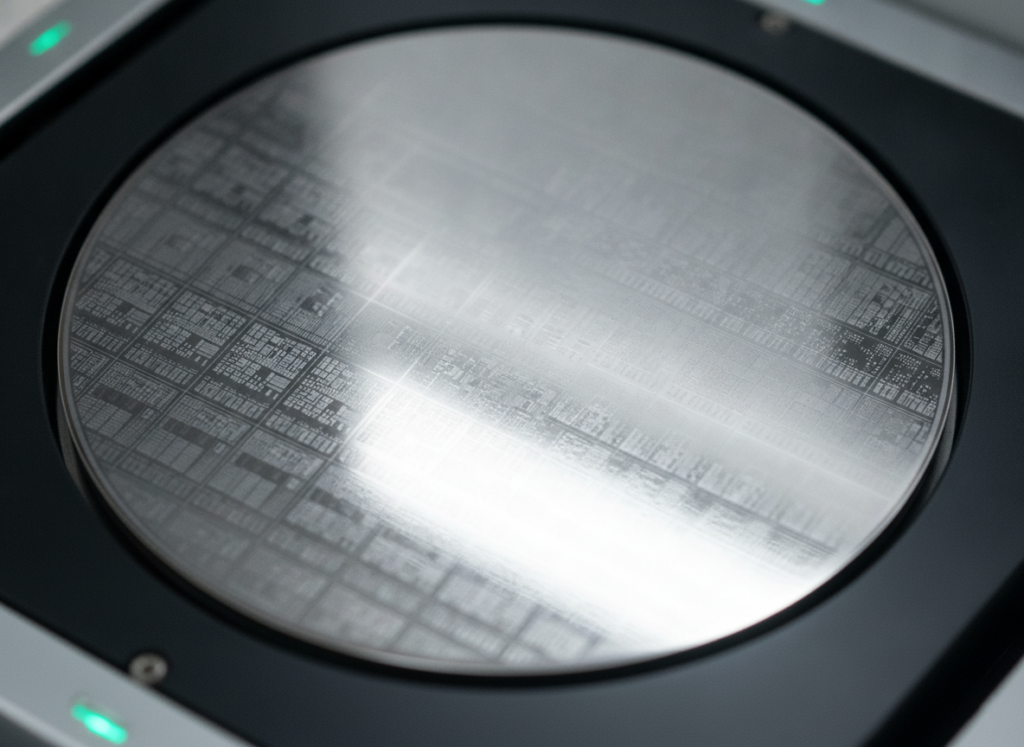
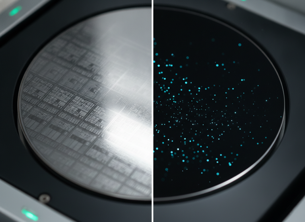
Bright-field inspection illuminates the wafer near-normal to the surface and collects the specularly reflected light. The surface comes back bright, and a defect that absorbs or disrupts that reflection appears as a dark feature against the bright background. It is the geometry closest to how a microscope images a surface, which is why it reads pattern detail so well.
That makes bright-field the tool for pattern defects on patterned wafers — bridges, opens, missing features, and other faults in the printed structure where contrast against the surrounding pattern is what you need. It resolves fine detail and gives an image an engineer can interpret directly.
The trade is that bright-field is comparatively slower, and it collects reflected light rather than scattered light. A small particle that scatters light at an angle bright-field never gathers can sit below its detection floor. The mode is not weak there — it is looking in the wrong direction for that defect.
Dark-field inspection turns the geometry around. It illuminates the wafer at a low, oblique angle and collects only the light that scatters off surface features. A clean surface reflects the illumination away from the detector and reads dark, while a particle or scratch scatters light back and lights up against that dark background.
That contrast is what makes dark-field fast and sensitive to particles, scratches, and surface contamination, especially on smooth or unpatterned wafers where there is little pattern to confuse the signal. It scans large numbers of wafers quickly, which suits inline particle monitoring.
What dark-field gives up is the detailed pattern image bright-field provides. It is built to flag scattering defects at speed, not to render the printed structure. Reach for it when the defect you fear is a particle on the surface, not a fault in the pattern — and the light source is where its sensitivity is actually decided.

This is the part most selection conversations underweight.
“I treated the dark-field light source as a brightness problem — more photons, more scattered signal, more particles caught. The physics corrected me. Scattering from a small particle scales with the inverse fourth power of wavelength, so moving to a shorter wavelength did more for small-particle sensitivity than doubling the power ever did. On the smallest particles that matter at advanced nodes, wavelength was the lever; brightness was a rounding error.” — metrology engineer, dark-field inspection development
For dark-field, wavelength is the dominant knob. Because scattered intensity from a small particle rises steeply as wavelength falls, a shorter-wavelength source — into the ultraviolet and deep ultraviolet — sharpens small-particle detection far more than added power does. That is why the most demanding dark-field tools push toward shorter wavelengths as defects shrink.
Bright-field asks something different of its source: uniform, stable illumination that holds imaging contrast across the field. A brighter source that is non-uniform or drifts does not help, because the result is an imaging measurement, not a scattering count. Matching the source to the mode — short-wavelength brightness for dark-field, uniform stability for bright-field — does more for results than any single headline number.
| Dimension | Bright-Field | Dark-Field |
|---|---|---|
| Illumination geometry | Near-normal, specular | Oblique, low-angle |
| Signal collected | Reflected light | Scattered light |
| Best for | Pattern defects on patterned wafers | Particles, scratches, surface defects |
| Surface suited to | Patterned | Smooth / unpatterned |
| Speed | Slower, high detail | Fast, high throughput |
| Light-source priority | Uniform, stable illumination | Short wavelength, high brightness |
| Blind spot | Low-angle scattering defects | Fine pattern detail |
The table shows two coverage maps, not two grades. Which leads to the failure mode worth naming before you commit.
“The cheaper tool ran a single inspection mode, and on paper it inspected every wafer. The hidden cost was the defect class it never reported. Pattern defects our bright-field caught were invisible to a dark-field-only neighbor tool, and the reverse held too — each mode had a blind spot the spec sheet didn’t mention. We learned it the expensive way, at a yield review, tracing escapes to a defect type no single mode could see. One inspection mode isn’t a cheaper version of two; it’s a different coverage map.” — yield engineer, fab inspection strategy
A single mode inspects every wafer and still misses an entire defect class, because the geometry that catches one type is the geometry that is blind to another. That is why many fabs combine both, and why treating bright-field vs dark-field wafer inspection as an either/or can cost more than the tool it saves. The right answer depends on which defects actually threaten your yield.

If your yield risk is pattern defects on patterned wafers, prioritize bright-field and a uniform, stable light source — detail and contrast are your binding constraints. If your risk is particles, scratches, or surface contamination, especially on smooth or unpatterned wafers, prioritize dark-field and weight the light-source wavelength above its raw power, since shorter wavelength is what lifts small-particle sensitivity.
If your defects of concern span both classes — and at advanced nodes they usually do — plan for both modes rather than forcing one to cover the gap. Match the illumination to the defect physics, then size brightness and resolution to the smallest defect you must catch. The mode that fits your dominant failure type is the one to build around first.
A few variables shift which mode matters most: whether your wafers are patterned or unpatterned, the size and type of the defects that threaten your yield, your throughput target, and how a new source has to integrate with an existing tool. Each one changes the answer.
Those details are hard to settle from a datasheet. If you are specifying inspection at scale, talking to an application engineer who has matched light sources to both modes can surface trade-offs no product listing will tell you.
The integrator who added a dark-field channel did not upgrade sensitivity — they closed a blind spot they could not see until a particle escaped. That is the quiet truth of inspection illumination: bright-field and dark-field are not better or worse, they are differently blind. The mode you leave out defines the defects you ship. Match the light to the defect, and coverage stops being a gamble.
What is the difference between bright-field and dark-field wafer inspection? Bright-field illuminates near-normal and collects reflected light, so defects appear dark against a bright background — good for pattern defects. Dark-field illuminates at a low angle and collects scattered light, so particles light up against a dark background — good for surface defects. They detect different defect classes.
Which is better, bright-field or dark-field inspection? Neither is universally better. Bright-field suits pattern defects on patterned wafers and high-resolution detail. Dark-field suits particles, scratches, and surface defects at high throughput. The right choice depends on which defects threaten your yield, which is why many fabs run both modes together.
Why is dark-field inspection more sensitive to particles? Dark-field collects light scattered by surface features against a dark background, which gives particles strong contrast. Its sensitivity rises sharply at shorter wavelengths, because scattering from a small particle scales with the inverse fourth power of wavelength, making wavelength the key light-source parameter for small-particle detection.
What light source does dark-field inspection need? Dark-field favors shorter-wavelength, high-brightness sources, often in the ultraviolet or deep ultraviolet. Because scattering increases steeply as wavelength falls, a shorter wavelength improves small-particle sensitivity more than added power does. Stability still matters, but wavelength is the dominant lever for dark-field performance.
Can one tool do both bright-field and dark-field inspection? Yes. Many inspection systems combine both modes to cover pattern defects and surface particles in one pass, since each mode has a blind spot the other covers. Running a single mode inspects every wafer but misses the defect class that mode cannot physically collect.
Is bright-field or dark-field faster? Dark-field is generally faster and suits high-throughput scanning of many wafers for particles and surface defects. Bright-field is slower but resolves fine pattern detail. The throughput difference is one reason fabs assign each mode to the defect type and inspection step it fits best.
Does bright-field inspection miss particles? It can. Small particles scatter light at angles a bright-field detector, positioned for specular reflection, never collects. Bright-field is not weak there — it is looking in the wrong direction for that defect. Catching those particles usually requires a dark-field channel.