For a decade, the through-silicon via was the obvious answer for 2.5D and 3D integration. The interesting part of the current shift is not that glass appeared — it is why packaging teams are switching to it, and the reason is rarely the one they walk in expecting.
“We evaluated glass interposers expecting the pitch to be cost — cheaper substrate, done. The number that actually moved our decision was insertion loss at high frequency. Silicon is a semiconductor, so even with an insulating liner the TSV path leaked signal as we pushed toward mmWave; the glass interposer’s native insulation cut that loss in a way silicon couldn’t follow. We came for the price and stayed for the electrical performance. TGV versus TSV wasn’t a cost trade — it was a frequency ceiling.” — packaging engineer, RF module development
I take that account seriously because it inverts the usual sales pitch. Glass gets marketed on cost, but the teams committing to it at advanced nodes are doing so for electrical reasons first. Understanding TGV vs TSV means looking past the substrate price to what each via does to a signal — and to where the real adoption bottleneck has been hiding.
TGV (through-glass via) interposers are rising over TSV (through-silicon via) mainly because glass is an insulator while silicon is a semiconductor. Glass has roughly a third of silicon’s dielectric constant and a loss tangent two to three orders of magnitude lower, which cuts RF insertion loss and signal coupling at high frequency. Glass also scales to large panels for better cost, and tunable-CTE glass can match the die. The historical obstacle was forming clean through-glass vias — a problem ultrafast laser processing now solves.
Heterogeneous integration and chiplets have made the interposer a performance component, not just a carrier. The substrate now decides how cleanly signals move between dies, how much power the interconnect wastes, and how far you can push frequency. That raises the stakes on a choice teams used to make by habit.
The driver underneath is frequency. 5G, mmWave, and high-speed digital links punish a lossy substrate, and silicon — being a semiconductor — carries loss and parasitic coupling that an insulating substrate avoids. As designs climb in frequency, the gap between a silicon interposer and a glass interposer stops being academic and starts showing up in the link budget.
Across advanced packaging work, I keep seeing the same realization: teams open the TGV vs TSV question expecting a cost spreadsheet and close it on an electrical argument. The sections below take each via apart — what silicon still does well, why through-glass via technology is gaining, and the via-formation problem that quietly gated glass for years.
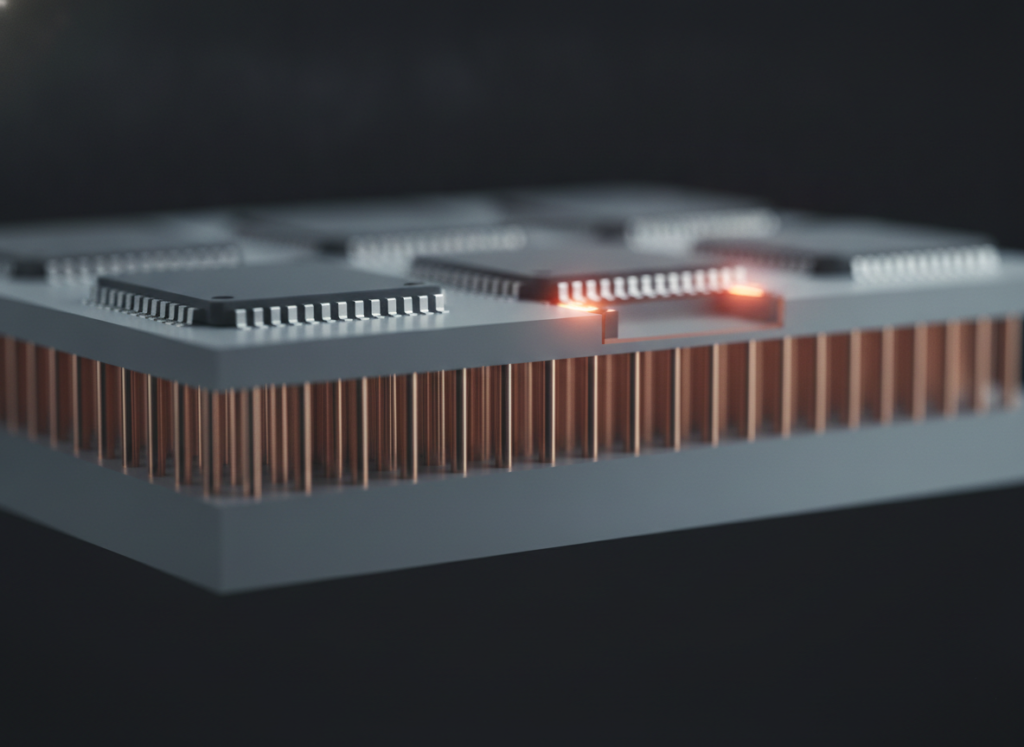
The through-silicon via earned its place. Silicon interposers ride a mature fab infrastructure, hit fine via pitch, and match the die’s coefficient of thermal expansion natively because the interposer and the chip are the same material. For dense, established 2.5D integration, TSV remains a strong default.
The strain shows at high frequency. Silicon is a semiconductor, so a TSV needs an insulating liner to keep signal in the conductor, and even then the substrate stays lossy. Its higher permittivity raises capacitance between neighboring vias, which makes via-to-via noise coupling worse than on glass. None of this disqualifies silicon — it just means the higher you push frequency, the harder the substrate works against you.
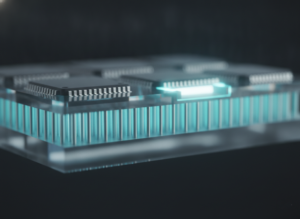
Glass starts from the opposite electrical position. It is an insulator, so a through-glass via does not fight the substrate to keep a signal clean. Glass carries roughly a third of silicon’s dielectric constant and a loss tangent lower by two to three orders of magnitude, which translates directly into lower RF insertion loss — reported as low as around 0.2 dB at 30 GHz for through-glass via coplanar lines in the literature.
That electrical advantage is why glass interposers are showing up first in RF front-ends, filters, and high-speed links, where loss is the binding constraint. Tunable-CTE glass also closes the old thermal-expansion objection, letting the substrate track the die more closely than its reputation suggests. The performance case, not the price tag, is what moved glass from research curiosity to roadmap.
Here is the part that stalled adoption longer than the physics warranted.
“We almost ruled glass out on reputation — brittle, CTE mismatch, cracks waiting to happen. Two of those three turned out to be solvable: tunable-CTE glass matched our die better than the silicon we were replacing. The one real obstacle was the via. Early drilled vias cracked and tapered, and that — not the glass itself — was what stalled the program. Once the through-glass vias were formed cleanly, with high aspect ratio and controlled taper, the brittleness argument evaporated. We’d been blaming the material for a process problem.” — R&D engineer, advanced packaging substrates
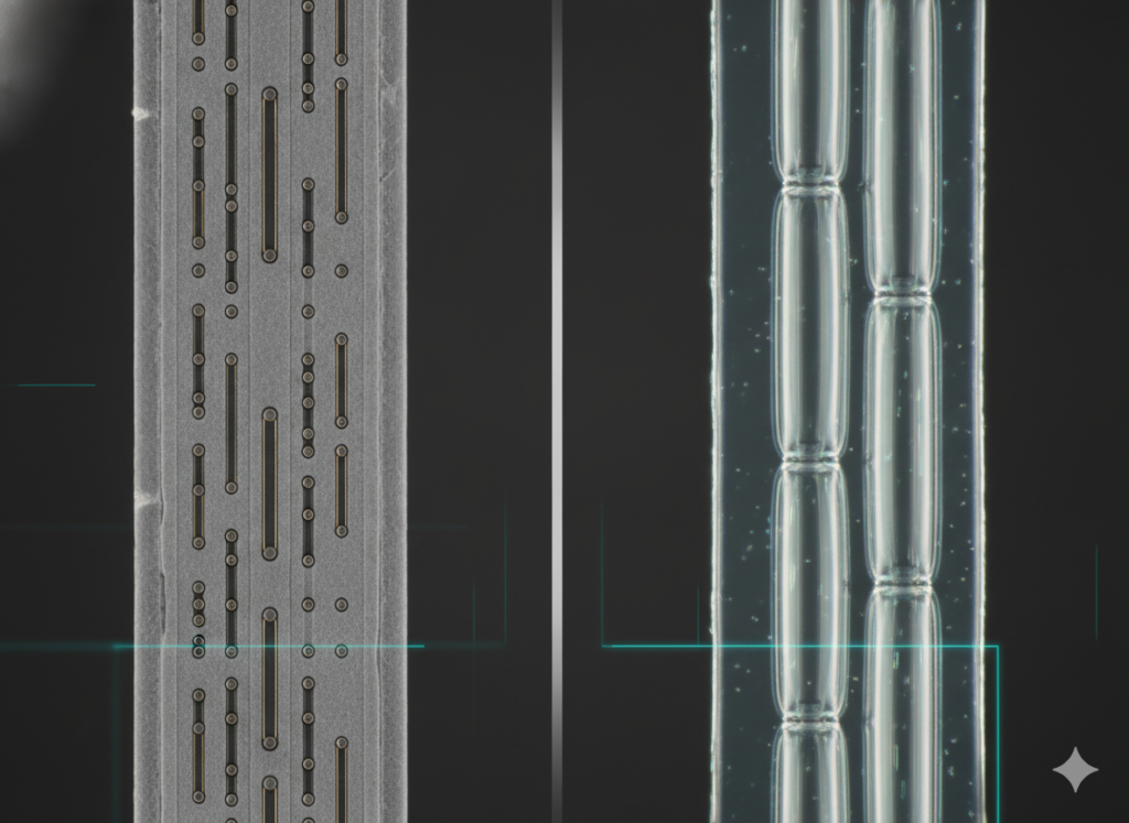
Glass is brittle, and a poorly formed via leaves stress that cracks it. For years that made through-glass via formation the practical barrier, not the electrical case. Ultrafast laser processing changed the equation: by removing material before heat spreads, it forms high-aspect-ratio vias — beyond 50:1 — with controlled taper in the 0–15° range and micron-level positional accuracy, without the micro-cracking that sank earlier attempts. When the via comes out clean and repeatable, the brittleness objection loses its force. The substrate was always ready; the hole was the holdup.

| Dimension | TSV (Silicon) | TGV (Glass) |
|---|---|---|
| Substrate nature | Semiconductor (needs liner) | Insulator (native) |
| Dielectric constant | Higher | ~1/3 of silicon |
| Loss tangent | Higher | 2–3 orders lower |
| RF insertion loss | Higher at high frequency | Low (≈0.2 dB at 30 GHz) |
| CTE match to die | Native | Tunable, can match |
| Panel scaling | Wafer-based | Large panels, better cost potential |
| Main obstacle | Substrate loss at high frequency | Clean via formation (laser-solved) |
The table frames the trade, but the cost story underneath it decides programs.
“On a per-wafer basis the silicon interposer looked competitive. The number that changed the business case was cost per good via at panel scale. Glass panels are large, so the via count per panel is enormous — and at that volume, via yield dominates everything else. A via process holding single-digit-ppm defects on glass turned a marginal cost case into a clear one, because the failures we weren’t scrapping were what used to sink the math. The interposer decision wasn’t made at the wafer; it was made at the via yield.” — manufacturing engineer, panel-level packaging
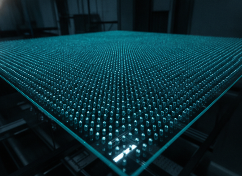
The economics of glass live at panel scale. Large panels carry enormous via counts, so the cost that matters is cost per good via, and via yield governs it. A formation process holding defects to single-digit ppm is what turns glass from a promising material into a manufacturable one. This is also where the laser via-formation story and the cost story converge: the same clean, repeatable via that solves brittleness is what protects yield at volume.
Worth a caution before the framework: glass is not a free win everywhere. At minimum pitch, interconnects on glass can show higher crosstalk than on silicon, so dense digital routing needs design attention rather than a blind swap.
If your design is RF, mmWave, or high-speed and loss is your binding constraint, glass interposers and through-glass via are likely the better path — the electrical margin is real and grows with frequency. If you are doing dense, established 2.5D integration at fine pitch where silicon’s maturity and crosstalk behavior matter more than substrate loss, TSV still earns its place. And if you are weighing the move at volume, run the numbers on cost per good via at panel scale, not per wafer, and confirm your via-formation process holds yield. Pick the via your signal and your panel economics actually need, not the one the industry defaulted to last decade.
A few variables shift the answer more than the substrate label: your operating frequency, your via pitch and density, your panel size and volume, and whether your via-formation process can hold aspect ratio and taper without cracking the glass. Each one changes where TGV pulls ahead of TSV.
Those details are hard to settle from a datasheet. If you are bringing a through-glass via process to volume, talking to an application engineer who has formed vias at production yield can surface trade-offs no product listing will tell you.
The team that came to glass for the price and stayed for the performance got the order of the argument right by accident. That is the quiet truth of TGV vs TSV: glass interposers are rising because an insulator beats a semiconductor where frequency is the constraint, and because the via that once cracked can now be formed clean. The substrate was never the hard part. The hole was — and that is solved.
What is the difference between TGV and TSV? TSV (through-silicon via) is a vertical interconnect through a silicon interposer; TGV (through-glass via) runs through a glass interposer. The core difference is the substrate: silicon is a semiconductor and lossy at high frequency, while glass is an insulator with much lower dielectric loss, giving TGV better RF performance.
Why are glass interposers replacing silicon? Mainly for electrical reasons. Glass has about a third of silicon’s dielectric constant and a far lower loss tangent, which cuts RF insertion loss and via-to-via coupling at high frequency. Glass also scales to large panels for better cost and can be tuned to match the die’s thermal expansion.
Is a glass interposer cheaper than a silicon interposer? It can be at scale. Glass comes in large panels with high via counts, so the figure that matters is cost per good via, where via yield dominates. With a high-yield via process, panel-scale glass can beat silicon on cost, though that depends on volume and process maturity.
What are the disadvantages of glass interposers? Glass is brittle, so via formation must avoid micro-cracking. At minimum pitch, glass interconnects can also show higher crosstalk than silicon, requiring design attention for dense digital routing. Silicon still leads in fab maturity and native CTE match to the die.
How are through-glass vias made? High-aspect-ratio through-glass vias are commonly formed with ultrafast laser processing, sometimes combined with etching. Ultrashort pulses remove material before heat spreads, producing vias beyond 50:1 aspect ratio with controlled taper and no micro-cracking, which is what made TGV manufacturable at production yield.
What applications use TGV technology? Through-glass via technology is used in RF front-end modules, filters and duplexers, mmWave packaging, MEMS and sensor packaging, and high-speed heterogeneous integration. These applications share a need for low insertion loss and good signal integrity, where glass outperforms silicon.
Does glass really have lower loss than silicon? Yes. Glass has a lower dielectric constant and a loss tangent two to three orders of magnitude below silicon’s, which reduces substrate loss and parasitics. Reported through-glass via coplanar lines show insertion loss around 0.2 dB at 30 GHz, supporting high-frequency signal transmission.
Is TGV ready for high-volume manufacturing? Increasingly, yes. The historical barrier was clean via formation, now addressed by ultrafast laser processing holding high aspect ratio and low defect rates. With via yield under control, glass interposers are moving from research into production roadmaps, especially for RF and high-speed applications.