Most teams I work with open the light-source decision by asking how much power they can get. It’s the wrong first question. In wafer defect inspection, the brightest source is rarely the one that finds the smallest defect — and the gap between that assumption and the physics is where inspection programs quietly lose sensitivity.
“The first build over-specified power on the assumption that a brighter source resolves more defects. It didn’t. On patterned wafers, the smallest defects we could repeatably separate from background were set by spectral purity, not watts. Moving to a source under 0.1nm linewidth — at lower average power — pulled features out of the noise that the higher-power, broader-linewidth unit had buried. Raw power was never the detection floor; linewidth was.” — process integrator, wafer defect-inspection light source selection
I take that account seriously because it repeats. Engineers scale the power axis because it is the easy number to compare on a datasheet, then find the detection floor was set by something else. Choosing a wafer defect inspection laser source well starts with knowing which specification actually moves your result, and which ones only add cost and thermal load.
The most important specification in a wafer defect inspection laser source is not power — it is spectral purity. A narrow linewidth, under 0.1nm, sets the resolution that separates real defects from background. Long-term output stability, rated in tens of thousands of hours, keeps your defect baseline trustworthy month over month. Power only matters until detection saturates. Prioritize wavelength selection for material absorption characteristics, linewidth for defect resolution, long-term output stability for baseline repeatability, and output mode (continuous or pulsed) for your inspection protocol; then size the power to the application rather than above it.
Inspection is the gate every wafer passes through, and the light source sits upstream of every decision the tool makes. Get the source wrong, and the cost does not show up as a failure — it shows up as bad data you trust. That is the expensive version of the mistake.
The stakes are not small. Inspection and metrology equipment account for a significant share of the semiconductor equipment market, and the pressure on defect detection sensitivity climbs with every node shrink. As feature sizes fall, the defects that matter get smaller than the assumptions built into older illumination setups.
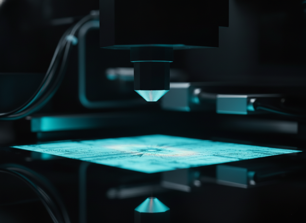
Across inspection light-source selections, the pattern I keep seeing is teams optimizing the specification that is easiest to quote instead of the one that governs the outcome. A wafer inspection light source has three parameters that decide whether the tool earns its place: how finely it resolves, how steadily it holds, and how uniformly it illuminates. The sections below take each in turn, then give you a framework to weigh them for your own line.
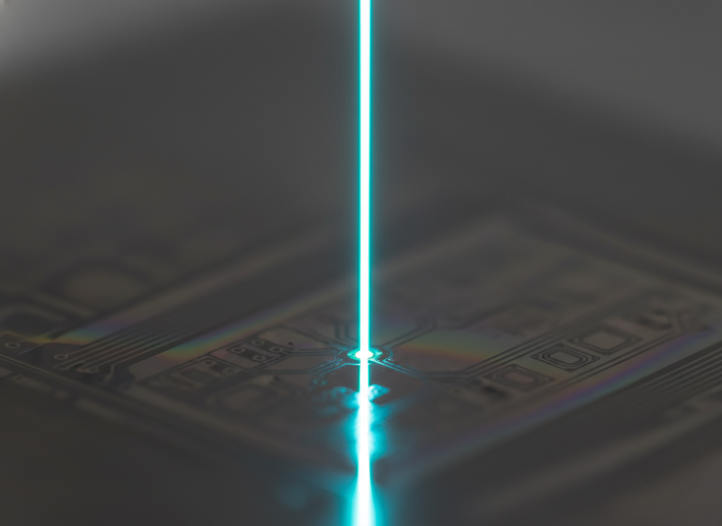
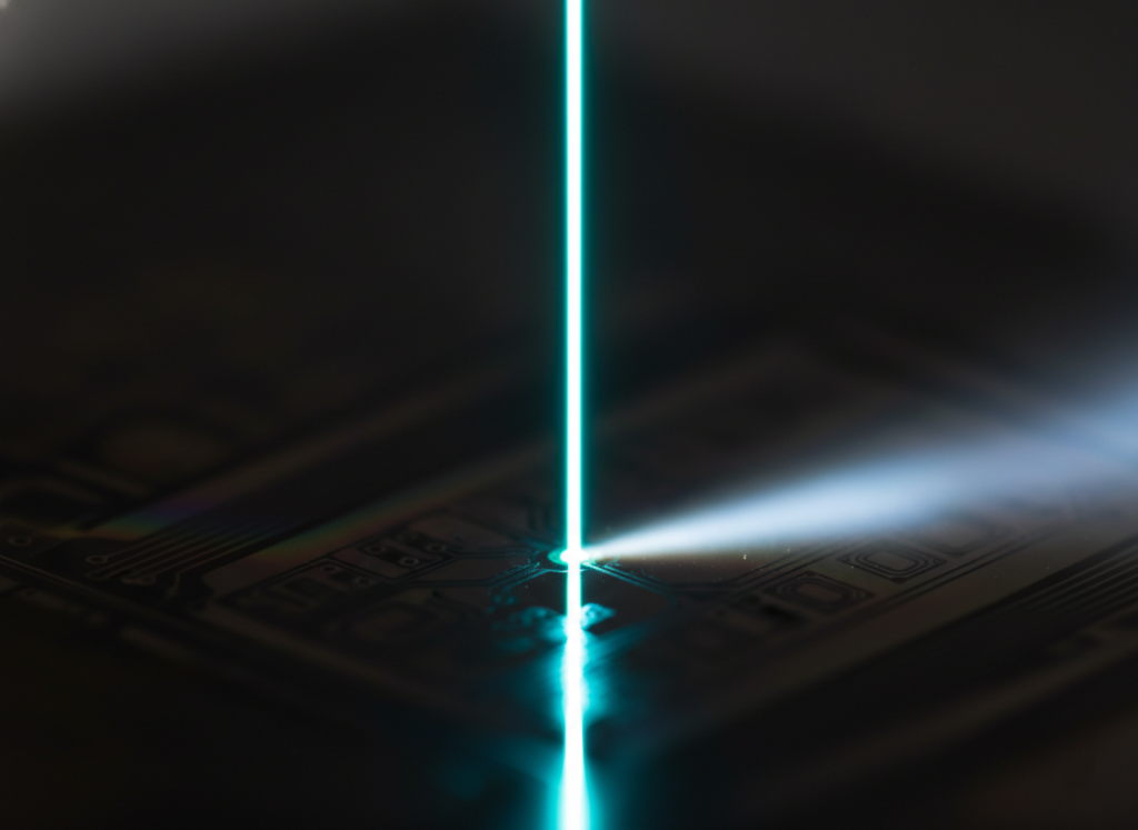
Linewidth is the width of the wavelength band the source emits. A narrow linewidth means the light is closer to a single, pure wavelength, which raises its coherence and, in turn, the resolution your optics can reach. That resolution is what lets the system separate a genuine defect from the background scatter around it.
This is the lever the integrator in the opening account missed. Past the point where detection saturates, adding watts does nothing for the smallest defect you can resolve — it just heats the optical train and raises cost. A source under 0.1nm linewidth pulls low-contrast features out of the noise that a brighter, broader-linewidth unit buries.
When you evaluate a wafer defect inspection laser source, ask for the linewidth specification before the power rating. If the supplier leads with watts and treats linewidth as a footnote, that ordering tells you something about what the source was built for.
Resolution gets the attention. Stability decides whether the numbers mean anything over time.
“The metric nobody quotes on a light-source datasheet is the one that hurts you in a fab: drift. Our first inspection source held spec on day one and wandered by week three. The tool didn’t fail — worse, it kept reporting, and the defect baseline drifted along with the source. We lost weeks chasing ‘process excursions’ that were really illumination drift. The replacement, rated for over 20,000 hours of stable output, dropped that false-excursion noise out of the data.” — metrology engineer, inline wafer defect inspection
A drifting source does not announce itself. The inspection tool keeps producing maps, and the shift in illumination reads as a shift in the wafers. Teams then spend weeks investigating excursions that were never on the wafer at all. When you judge long-term stability, look for output stability rated across tens of thousands of hours, not a day-one figure. The detection sensitivity you qualify on installation is only useful if the source still holds it next quarter.
If you are weighing two sources with similar linewidth, stability is usually the tiebreaker worth paying for.
Inspection and material processing ask opposite things of a laser,inspection and material processing ask opposite things of a laser, and reusing the wrong one not only costs a design cycle but introduces defect-escape risk.
“We defaulted to a pulsed source because that’s what our processing lines ran. For inspection, it fought us — pulse-to-pulse variation showed up as illumination non-uniformity across the field, and we burned integration time averaging it out. A near-continuous source at 80–120MHz gave effectively uniform illumination and let us shorten inspection cycle time without losing sensitivity.” — light-source engineer, inspection equipment OEM
A processing laser concentrates energy in widely spaced pulses to ablate material. Inspection wants the opposite: steady, uniform light across the field so the camera sees an even scene. A source running at a near-continuous repetition rate of 80–120MHz behaves, for imaging purposes, like continuous illumination — which removes the pulse-to-pulse variation you would otherwise average out at the cost of throughput. When the goal is uniform light rather than concentrated energy, output mode stops being a detail.
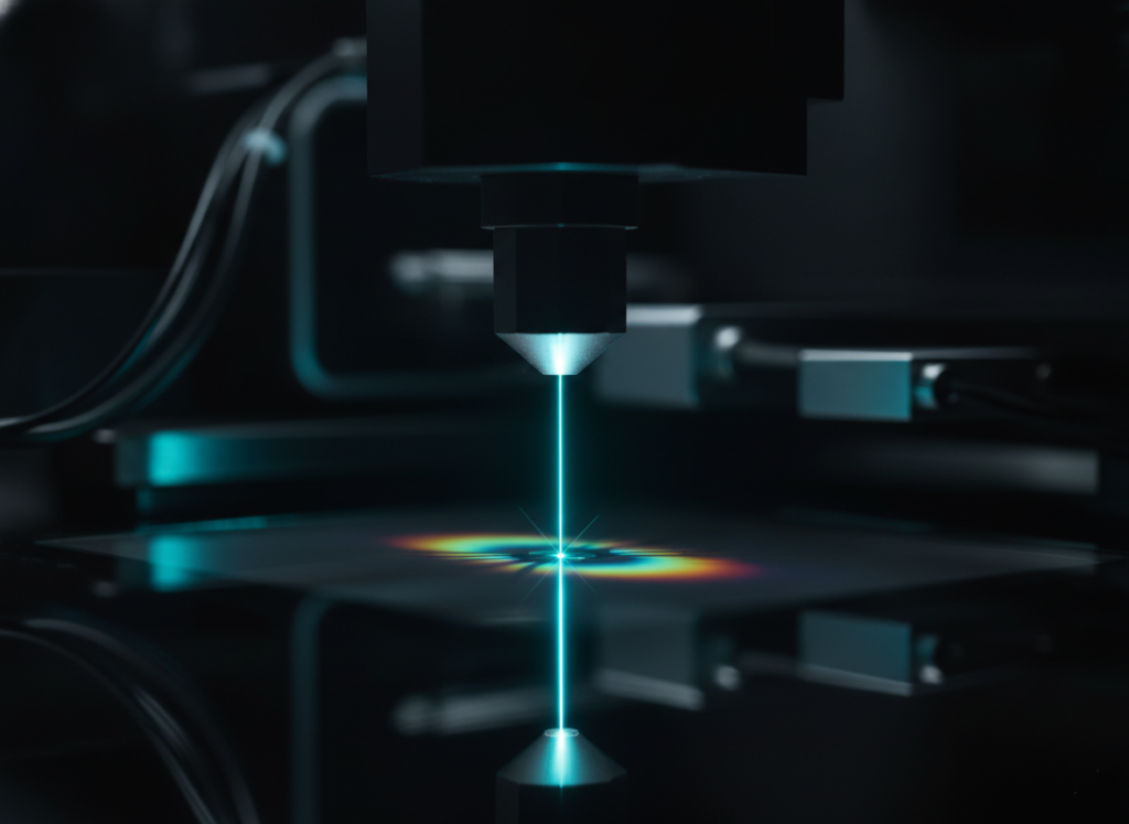
Wavelength sets the smallest defect the system can see. Shorter wavelengths, into the ultraviolet and deep ultraviolet, resolve smaller features, which is why the most demanding inspection tasks push toward shorter wavelengths as nodes shrink. The trade is real: shorter wavelengths demand more from the optics and raise system cost, so the right choice depends on your defect-size target rather than a blanket “shorter is better.”
Wavelength also interacts with how you illuminate. Bright-field inspection, with light reflected near-normal to the surface, suits detailed pattern-defect review, while dark-field inspection collects scattered light at a low angle and runs fast across many wafers. Matching wavelength and illumination geometry to your defect type does more for results than chasing any single headline number.
| Dimension | What it controls | What to look for | Failure mode if wrong |
|---|---|---|---|
| Linewidth | Resolution / detection floor | Narrow, under 0.1nm | Smallest defects buried in background |
| Stability | Data trust over time | Rated across tens of thousands of hours | False excursions, untrustworthy yield data |
| Output mode | Illumination uniformity | Near-continuous (high rep rate) | Non-uniform field, longer inspection time |
| Wavelength | Smallest visible defect | Matched to defect-size target | Over- or under-resolved for the node |
That table is the short version of every selection conversation I have. Before you map it onto your line, one framework helps.
If you inspect patterned wafers and need the smallest possible defects, prioritize linewidth first and wavelength second — resolution is your binding constraint. If you run inline monitoring in a fab where the source operates for months, weight long-term stability and lifetime above a marginal sensitivity gain, because data you cannot trust over time is not data. If your throughput is limited by illumination non-uniformity, look hard at output mode and reach for a near-continuous source.
In every case, size power to the point where detection saturates, then stop. Power past that point buys cost and heat, not sensitivity. Pick the source that wins on the axis your application is actually bound by — not the one with the largest number on the front of the datasheet.
A few variables decide more than the source specification alone: your target defect size, whether your wafers are patterned or non-patterned, whether you run bright-field or dark-field, and how the source has to integrate with an existing inspection tool. Each one shifts which parameter matters most.
Those details are hard to settle from a datasheet. If you are sourcing at scale, talking to an application engineer who has matched sources to inspection tools can surface trade-offs no product listing will tell you.
The integrator who stopped scaling power did not lower the bar. They found the axis the result was actually bound by, and spent their budget there. That is the quiet truth of wafer inspection: the brightest source is not the one that finds the defect, and the source you can trust six months from now matters more than the one that looked best on installation day. Match the light to the wafer, not to the spec sheet, and the rest follows.
What is the most important spec in a wafer defect inspection laser source? The most important specs work together: wavelength (material absorption), output mode (illumination uniformity—favor near-continuous over pulsed), stability (month-to-month baseline reliability), and linewidth (<0.1nm for defect resolution). These four factors determine whether you can separate real defects from noise. Power is secondary—it matters only until detection saturates, after which extra watts add cost and heat without improving detection sensitivity.
Does higher power improve defect detection? Only up to a point. Once detection saturates, more power does not help you resolve smaller defects — it adds thermal load to the optical train and raises cost. Beyond saturation, linewidth, stability, and wavelength govern detection sensitivity far more than raw power does.
What wavelength is best for wafer defect inspection? Shorter wavelengths, into the ultraviolet and deep ultraviolet, resolve smaller defects, which suits advanced nodes. The trade-off is higher optical complexity and cost. The best wavelength depends on your target defect size rather than a blanket rule, so match it to the smallest defect you need to catch.
Should an inspection light source be pulsed or continuous? Ideally, continuous illumination. Continuous light delivers perfect uniformity across the field with zero pulse-to-pulse variation. As continuous inspection sources mature, near-continuous repetition rates of 80–120MHz serve as the current best alternative—they behave effectively like continuous light while pulsed processing-grade sources introduce field non-uniformity that requires expensive integration-time averaging to correct.
How does light-source stability affect yield data? Poor long-term stability causes the source to drift across its operational lifetime, gradually shifting the defect baseline without triggering failure alarms. The tool keeps reporting normally, but baseline drift reads as wafer excursions, sending teams to chase non-existent process problems. A stable light source maintains consistent optical output across tens of thousands of hours of operation, keeping defect baselines reliable throughout the tool’s service life.
What is the difference between bright-field and dark-field inspection? Bright-field illumination reflects light near-normal to the surface and suits detailed pattern-defect review. Dark-field collects scattered light at a low angle, runs fast across many wafers, and works well on reflective surfaces. Many environments combine both to raise inspection confidence.
How long should an inspection light source hold its output? Look for output stability rated across tens of thousands of hours, not a day-one figure. Inline inspection sources run continuously for months, and the detection sensitivity qualified at installation only matters if the source still holds it through the quarter.