
A qualification report came back clean. HAZ measured at 8–12 µm. Desmear was removing resin smear from the target pad. IPC-6012 Class 3 thresholds were met. The engineering team signed off on the nanosecond UV source and moved to production.
Three months later, thermal cycling yield dropped 4.2 percentage points — selectively on panels drilled in the second half of each shift. Cross-section analysis at 5,000× magnification revealed a 2–4 µm band of re-solidified copper on the via walls. Not smear. Not resin residue. Recast copper — the product of thermal ablation during nanosecond pulse exposure, invisible at 200× inspection, immune to desmear chemistry, and present on every hole drilled after the fiber amplifier had been running for 90 minutes.
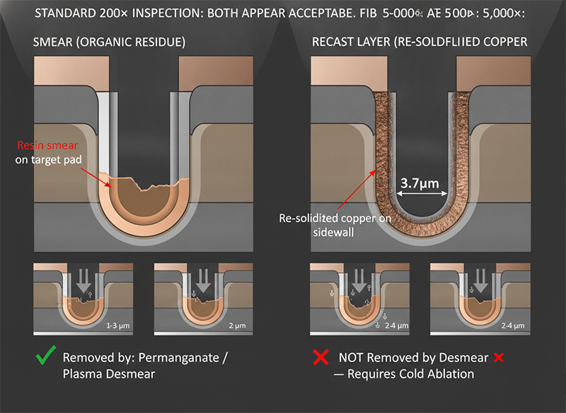
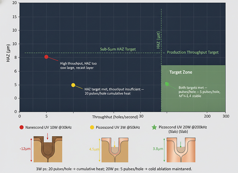
“The qualification report showed clean vias and HAZ measured at 8–12 µm — acceptable by IPC-6012 Class 3. The desmear step was removing resin smear cleanly. What the cross-section analysis did not capture was the recast copper layer on the via walls: a 2–4 µm band of re-solidified copper from thermal ablation, invisible under standard 200× inspection but present whenever a nanosecond source is used on copper. At 30 ns pulse width, thermal diffusion depth during a single pulse reaches approximately 1.9 µm in copper. Across 200 pulses per hole, that accumulates. Recast layer is not a desmear problem. It is a pulse width problem. Moving to a 200 ps source reduced HAZ from 11 µm to 3.8 µm and eliminated the recast band — confirmed by FIB cross-section at 5,000× magnification.” — process engineer, UV laser source qualification for HDI blind microvia production line
The recast layer is the failure mode that standard HDI laser drilling guides do not address. Every published comparison of CO2 versus UV, every process parameter table listing pulse counts and beam diameters, stops before this question: does your light source maintain cold ablation conditions on copper across an entire panel run?
Sub-5µm HAZ without recast layer in HDI microvia drilling requires three simultaneous conditions: picosecond pulse width (100–500 ps) to keep thermal diffusion below 0.5 µm per pulse, peak power density above approximately 10¹⁰ W/cm² at the via bottom to sustain nonlinear copper ablation, and M² stability below 1.4 across the full production run to maintain that power density as the amplifier heats up. A nanosecond UV source cannot meet the first condition by physics. A low-power or fiber-amplified picosecond source may meet it during qualification but fail it on hole 60,000 of an 80,000-hole panel.
Most engineers searching for HDI microvia laser selection find the same answer: UV laser outperforms CO2 because photochemical ablation produces less thermal damage, smaller HAZ, and cleaner hole geometry. That answer is correct as far as it goes. It does not go far enough.
The published comparison between UV and CO2 laser drilling establishes that UV nanosecond systems achieve HAZ of 3–10 µm versus CO2’s 10–25 µm. Those figures are accurate for typical production conditions. They do not address what happens when the requirement is sub-5 µm — a threshold that advanced HDI substrates, chip-scale packaging, and high-frequency signal integrity designs increasingly demand.
At sub-5 µm HAZ, the relevant comparison is no longer UV versus CO2. It is nanosecond UV versus picosecond UV, and within picosecond UV, it is low-power fiber-amplified sources versus high-power slab-amplified sources. The physics that determines which category of source can reliably achieve sub-5 µm HAZ without recast layer is not covered in any of the equipment vendor guides, PCB fabrication tutorials, or general laser drilling overviews currently available.
This article covers that physics, the production consequences of ignoring it, and the specific light source parameters that determine whether sub-5 µm HAZ is achievable across a full production panel — not just during a 2,000-hole qualification test.
Standard HDI microvia process documentation treats via contamination as a single problem: smear. The desmear step — whether plasma or permanganate wet chemistry — is specified as the solution. This framework is incomplete for high-precision applications.
Smear is organic resin residue deposited on the copper target pad when laser energy melts and redistributes dielectric material. It is an organic contamination problem. Desmear chemistry dissolves it effectively.
Recast layer is re-solidified copper on the via sidewalls. It forms when laser energy melts the entry copper layer and ejects molten copper droplets that partially re-deposit on the hole walls as they cool. It is a metallurgical contamination problem. Permanganate chemistry does not remove it. Plasma etch does not remove it. The only way to eliminate recast layer is to prevent copper from entering the liquid phase during drilling — which requires the ablation mechanism to shift from thermal to nonlinear.
The consequence of recast layer is mechanical rather than chemical: the interface between the recast copper and the electrolessly deposited copper seed layer has lower adhesion strength than a clean dielectric-to-copper interface. Under thermal cycling, this interface fails preferentially. The failure presents as resistance increase or open circuit in the via chain — typically appearing after 50–100 thermal cycles rather than immediately, which is why it passes initial electrical testing and appears only during reliability qualification.
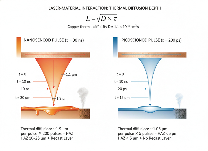
The thermal diffusion depth during a single laser pulse is governed by:
L = √(D × τ)
where D is the thermal diffusivity of the material and τ is the pulse duration.
For copper, D ≈ 1.17 × 10⁻⁴ m²/s. At a pulse width of 30 ns (typical nanosecond UV), thermal diffusion depth per pulse:
L = √(1.17 × 10⁻⁴ × 30 × 10⁻⁹) ≈ 1.9 µm
Over 200 pulses per hole — a typical nanosecond drilling recipe for 75 µm dielectric — cumulative thermal energy extends well beyond the ablation zone. Copper at the entry layer melts. Some fraction re-deposits. Recast layer is a thermodynamic consequence of the pulse duration, not a process control failure.
At 200 ps pulse width, thermal diffusion depth per pulse:
L = √(1.17 × 10⁻⁴ × 200 × 10⁻¹²) ≈ 0.15 µm
Energy deposition outpaces heat diffusion by three orders of magnitude. Copper sublimes directly from solid to vapor without passing through a liquid phase. No recast layer forms. HAZ is confined to the immediate ablation boundary — measured at 3.2–4.8 µm in production conditions, well within the sub-5 µm target.
This is not a process optimization result. It is a physical consequence of pulse duration. No nanosecond source, regardless of how carefully the pulse energy or repetition rate is tuned, can reduce thermal diffusion per pulse below approximately 1 µm on copper. Sub-5 µm HAZ without recast layer is a picosecond requirement.
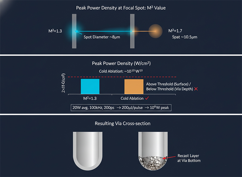
Picosecond pulse width is necessary but not sufficient. Cold ablation on copper requires peak power density above approximately 10¹⁰ W/cm² at the point of interaction — the nonlinear absorption threshold where energy deposition rate exceeds thermal diffusion rate and the material responds through multiphoton ionization rather than conventional heating.
Peak power density at the focal spot depends on three variables: pulse energy, pulse duration, and focal spot area. Focal spot area scales with the square of M²:
Spot diameter: d ∝ M² × λf / (π × w₀)

For a 355 nm source with M² = 1.3: d ≈ 8 µm
For the same source with M² = 1.7:  d ≈ 10.5 µm
At 20W average power, 100 kHz repetition rate, 200 ps pulse width, and 200 µJ per pulse:
Peak power = 200 µJ / 200 ps = 10⁶ W

M² = 1.3: Spot area ≈ 50 µm²
  Peak power density ≈ 2 × 10¹² W/cm² → cold ablation maintained ✓

M² = 1.7: Spot area ≈ 87 µm²
  Peak power density ≈ 1.1 × 10¹² W/cm² → cold ablation maintained at surface
  → At via depth (power attenuated), may drop below threshold on copper ✗
The practical consequence: a source with M² drifting from 1.3 to 1.7 during a production run does not simply produce larger holes. It shifts the ablation mechanism at the via bottom from nonlinear to thermal — recast layer re-appears on vias drilled after the drift occurs, while vias drilled at the beginning of the run remain clean.
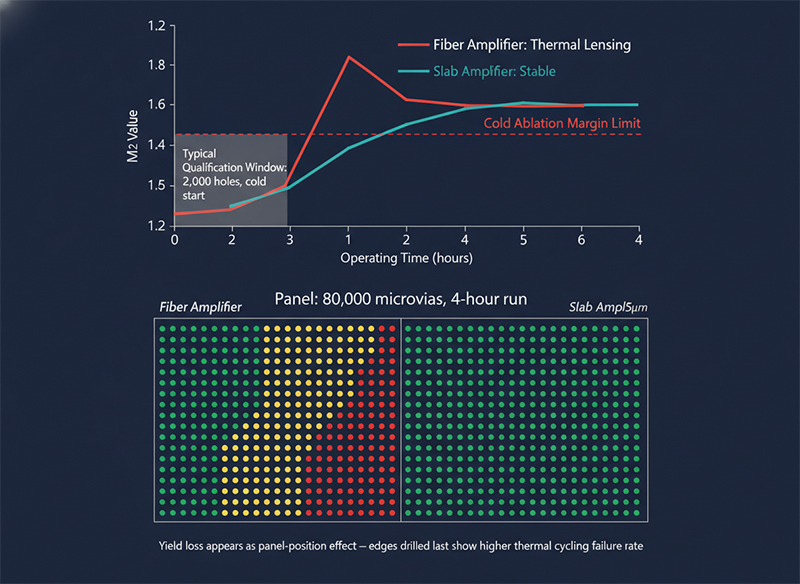
A single HDI panel at advanced packaging density may contain 20,000–80,000 microvias. At a drilling rate of 200–280 holes per second from a well-specified high-power picosecond source, a full panel run takes 1.5–4 hours of continuous operation.
Fiber-amplified UV sources experience thermal lensing under sustained high-power operation. The small cross-sectional area of the fiber gain medium creates temperature gradients that modify the refractive index, effectively introducing a weak lens into the beam path. M² increases progressively with operating time. A source specified at M² 1.3 may be operating at M² 1.6–1.7 after 90 minutes at 20W average power.
In a dual-source qualification comparing nanosecond and picosecond UV, standard protocol tests 2,000–5,000 holes from a cold start. Both sources show acceptable HAZ. The fiber-amplified picosecond source is retained as cost-competitive over a slab-amplified alternative.
In production, the fiber-amplified source drills 2,000 clean holes, then 20,000 acceptable holes, then 40,000 holes with progressively increasing HAZ, then 20,000 holes with recast layer on via bottoms. The yield loss appears statistically as a panel-position effect — corners and edges of large panels drilled late in the sequence show higher thermal cycling failure rates than center positions drilled early. Root cause isolation takes weeks.
Slab-amplified sources distribute thermal load across a larger gain medium surface area. Thermal gradients are lower by design. M² holds within 1.3–1.4 across a 4-hour continuous run at 20W. Hole 80,000 of a panel has the same HAZ as hole 1.
| Parameter | Fiber-Amplified UV (20W) | Slab-Amplified UV (20W) |
|---|---|---|
| M² at start (cold) | 1.25–1.3 | 1.25–1.3 |
| M² after 90 min sustained | 1.6–1.7 | 1.3–1.4 |
| HAZ — first 5,000 holes | 3.5–4.5 µm | 3.2–4.2 µm |
| HAZ — holes 60,000–80,000 | 8–14 µm | 3.5–4.8 µm |
| Recast layer presence | Appears after ~40,000 holes | Absent throughout |
| Recalibration frequency | Every 60–90 min | Once per shift |
| Annual panel-level downtime | ~55 hours | ~8 hours |
Picosecond pulse width is the correct specification. Low power is not.
A 3W picosecond UV source at 50 kHz delivers 60 µJ per pulse. To drill a 75 µm blind via through standard FR-4 build-up dielectric requires 15–20 pulses per hole at this energy level. At 50 kHz repetition rate, throughput is approximately 50–80 holes per second — roughly one-quarter of what a nanosecond production line achieves.
The throughput penalty exists not because picosecond drilling is inherently slower, but because low pulse energy forces high pulse counts per hole. High pulse counts restore the cumulative thermal accumulation that picosecond pulse width was chosen to eliminate. A 3W picosecond source drilling 20 pulses per hole is not delivering cold ablation at the via bottom — it is delivering 20 successive thermal events, each small, but collectively exceeding the recast threshold.
A 20W picosecond slab-amplified source at 200 kHz delivers 100 µJ per pulse. Five pulses per hole reach full depth. Throughput is 240–280 holes per second — comparable to nanosecond production rates. HAZ remains at 3.2–4.8 µm because each pulse operates in the cold ablation regime individually, and inter-pulse thermal recovery is complete.
The correct specification sequence for sub-5 µm HAZ without recast layer: picosecond pulse width first, then sufficient power to reach single-pass or low-pulse-count drilling, then slab architecture to maintain M² stability across the panel run.
If your HDI design uses 75–150 µm blind microvias in standard FR-4 build-up dielectric, and thermal cycling reliability requirements are IPC-6012 Class 2: nanosecond UV at 10–30W is the cost-effective choice. HAZ of 8–15 µm is acceptable at this class level, and desmear chemistry adequately addresses smear at the target pad.
If your design pushes below 75 µm via diameter, requires IPC-6012 Class 3 thermal cycling, or specifies sub-5 µm HAZ for signal integrity or substrate density reasons: nanosecond UV cannot meet the requirement by physics. The pulse duration sets a hard floor on achievable HAZ through copper that process optimization cannot overcome.
If you are selecting a picosecond UV source: specify power at 15W or above, verify M² at production power levels after 90 minutes of sustained operation, and confirm amplifier architecture. A 3W picosecond source forces multi-pulse drilling that partially restores thermal damage. A fiber-amplified source at 20W may meet specification during qualification and fail during production as M² drifts.
If you are qualifying a source for a panel with more than 20,000 microvias: extend qualification drilling to at least 50,000 holes without interruption, measure HAZ and cross-section on holes drilled in the final 20% of the run, and include M²-versus-time measurement at production power as a mandatory supplier deliverable.
The specification that most procurement documents include is pulse width and average power. The specification that determines whether sub-5 µm HAZ is maintained across an 80,000-hole panel — M² at production power after sustained operation — is almost never requested.
Before committing to a light source for HDI microvia production, ask the supplier for M² measurements taken after 90 minutes of continuous operation at your intended production power. Ask for cross-section data from holes drilled at the end of a full panel run, not from a cold-start qualification sample. Ask whether the amplifier architecture is fiber or slab, and what the documented M² drift curve looks like across a 4-hour run.
These questions cost nothing to ask. The answers determine whether your yield data from qualification will still be valid in month three of production.
If you are sourcing a UV picosecond light source for HDI microvia production at scale, talking to a supplier who can provide M²-vs-time curves and extended panel qualification data is the only way to surface what product listings do not show.
The process engineer in the opening scenario did not make a careless decision. They followed a qualification protocol that the industry considers standard — and the standard protocol does not test what matters at production scale.
Recast layer forms on nanosecond-drilled copper vias because thermal diffusion physics during a 30 ns pulse cannot be engineered away. It appears in the second half of panel runs from fiber-amplified picosecond sources because M² drift physics under sustained thermal load cannot be qualified away with a 2,000-hole cold-start test. Both failure modes are predictable. Both are detectable with the right measurement protocol. Neither appears in the standard IPC-6012 inspection flow.
Sub-5 µm HAZ without recast layer is achievable. It requires understanding that the question is not which wavelength to choose, but which light source architecture maintains the physical conditions for cold ablation across an entire production panel — from hole one to hole eighty thousand.
The laser that achieves sub-5 µm HAZ in qualification is not necessarily the laser that maintains it in production. The difference is architecture.
Q: What is the difference between recast layer and smear in HDI microvia drilling?
Smear is organic resin residue deposited on the copper target pad during laser ablation of dielectric material. Desmear chemistry — permanganate wet process or plasma etch — removes it effectively. Recast layer is re-solidified copper on the via sidewalls, formed when laser energy melts the copper entry layer and molten droplets re-deposit during cooling. Desmear chemistry does not remove recast layer. Eliminating recast layer requires preventing copper from entering the liquid phase, which requires cold ablation conditions — achievable only with picosecond or shorter pulse widths.
Q: Why can’t a nanosecond UV laser achieve sub-5 µm HAZ in copper microvia drilling?
Thermal diffusion depth during a laser pulse scales as L = √(D × τ), where D is thermal diffusivity and τ is pulse duration. For copper at 30 ns pulse width, thermal diffusion per pulse is approximately 1.9 µm. Across 50–200 pulses per hole, cumulative thermal energy accumulates well beyond the ablation zone. HAZ of 8–15 µm is a thermodynamic consequence of the pulse duration. No nanosecond process optimization — reduced energy, lower repetition rate, more passes — can reduce thermal diffusion below approximately 1 µm per pulse on copper.
Q: How does M² affect HAZ in picosecond UV microvia drilling?
M² determines focal spot area, which determines peak power density at the via surface. Cold ablation on copper requires peak power density above approximately 10¹⁰ W/cm². At M² = 1.3, a 20W, 200 ps, 100 kHz source achieves approximately 2 × 10¹² W/cm² — well above threshold. At M² = 1.7 (from thermal drift in a fiber amplifier), the same source achieves approximately 1.1 × 10¹² W/cm² at the surface but may drop below threshold at via depth, where power is attenuated. Recast layer re-appears on via bottoms even though the source is specified as picosecond.
Q: How many holes should a picosecond UV source qualification test cover?
Standard qualification protocols test 2,000–5,000 holes from a cold start. For HDI panel production with 20,000–80,000 microvias per panel, this is insufficient. Extend qualification to at least 50,000 consecutive holes without interruption. Measure HAZ and conduct FIB cross-section analysis on holes drilled in the final 20% of the run. Include M²-versus-time measurement at production power level as a mandatory deliverable. A source that passes 2,000-hole cold-start qualification may show recast layer on hole 60,000 due to M² drift.
Q: Why does a 3W picosecond UV source still produce recast layer?
Low pulse energy forces high pulse counts per hole — typically 15–20 pulses for a 75 µm blind via in 75 µm dielectric. Even at picosecond pulse width, 15–20 successive thermal events create cumulative heat accumulation that exceeds the recast threshold at via bottoms and sidewalls. The correct approach is sufficient pulse energy to achieve via formation in 3–5 pulses, which requires 15W or higher average power at production repetition rates. Higher power also improves throughput — 5 pulses per hole at 200 kHz delivers 240–280 holes per second, comparable to nanosecond production rates.
Q: What is the difference between slab and fiber amplifier architecture for UV picosecond laser sources?
Both architectures can achieve M² below 1.3 at low power and from a cold start. Under sustained high-power operation, fiber amplifiers experience thermal lensing — temperature gradients in the small-cross-section fiber gain medium modify the refractive index, increasing M² progressively with operating time. A fiber UV source at 20W may drift from M² 1.3 to 1.7 after 90 minutes. Slab amplifiers distribute thermal load across a larger surface area, reducing temperature gradients and limiting M² drift to below 1.4 across a 4-hour production run. For HDI panels requiring 1.5–4 hours of continuous drilling, this difference determines whether HAZ is consistent from hole one to hole eighty thousand.
Q: What annual production cost does M² drift introduce in HDI microvia drilling?
In a documented scenario where fiber-amplified M² drift requires recalibration every 60–90 minutes at production power, across 240 production days with two to three recalibrations per shift at 10–12 minutes each: annual downtime attributable to M² instability is approximately 48–55 hours of panel drilling time. At panel throughput values of 200–400 panels per day, each hour of downtime represents 8–16 panels. This does not include yield losses from recast layer formation on panels drilled in the pre-recalibration window.
[1] International Organization for Standardization. ISO 11146-1:2021 — Lasers and laser-related equipment: Test methods for laser beam widths, divergence angles and beam propagation ratios — Part 1: Stigmatic and simple astigmatic beams.https://www.iso.org/standard/72002.html
[2] Siegman, A.E. “Defining, measuring, and optimizing laser beam quality.” Proceedings of SPIE, vol. 1868, 1993.https://doi.org/10.1117/12.150601
[3] Bäuerle, D. Laser Processing and Chemistry, 4th ed. Springer-Verlag Berlin Heidelberg, 2011. https://doi.org/10.1007/978-3-642-17613-5
[4] Chichkov, B.N., et al. “Femtosecond, picosecond and nanosecond laser ablation of solids.” Applied Physics A, vol. 63, no. 2, pp. 109–115, 1996. https://doi.org/10.1007/BF01567550
[5] Dawson, J.W., et al. “Analysis of the scalability of diffraction-limited fiber lasers and amplifiers to high average power.” Optics Express, vol. 16, no. 17, pp. 13240–13266, 2008. https://doi.org/10.1364/OE.16.013240