
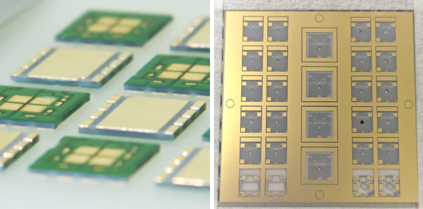
△ Ceramic PCB Material Display
Aluminum nitride (AIN) ceramic PCBs , with their excellent characteristics of high thermal conductivity and high insulation, are widely used in AI optical modules , semiconductors, automotive electronics, and other high-end fields. The substrate adopts a ceramic-metal composite structure; traditional mechanical cutting easily causes defects such as chipping and micro-cracks, making it difficult to meet the stringent requirements of mass production at the micrometer level.
This article is based on ultraviolet picosecond laser cutting specialized process verification , delivering practical process solutions and measured results to provide technical references for precise cutting of thin aluminum nitride PCBs.
Aluminum nitride ceramic substrates have high density and brittleness; the processing process is highly sensitive to mechanical stress and thermal input, and even slight deviations in the process can damage the substrate matrix and metal traces. The ultraviolet picosecond laser relies on the mechanism of ultra-short pulse cold processing , requiring no external force to fracture the material; instead, it uses pulsed energy to instantly vaporize and peel off the material, thereby aligning with the processing conditions of such hard and brittle composite substrates from a fundamental mechanistic perspective. The core technological advantages are as follows:
It focuses light spots at a micron scale, has precise trajectory control, can process tiny high-density graphs, and has no machining bias or deformation problems.
The small cut width reduces substrate loss and reduces volume production costs.
It inhibits heat diffusion, avoids yellowing, carbonization and deformation, and the insulation and thermal conductivity of the substrate are not destroyed.
The whole process is non-contact processing, there is no squeeze shock, and significantly reduces cracks, cracks, and layering, suitable for large-scale production.
To verify the adaptability and process stability of ultraviolet picosecond laser on aluminum nitride PCBs, Huachuang Hongdu conducted specialized process testing, selecting samples of 0.28 mm thin aluminum nitride ceramics PCB ,From processing precision , thermal effects , and edge quality across multiple dimensions, evaluate process stability to establish reusable process reference standards.The practical core process data and machining effect verification are as follows:
The overall positioning accuracy of the system reaches ±2μm, combined with high-speed galvanometer trajectory control, avoiding mechanical machining-induced deformation。Based on the measured material thickness of 0.28 mm: the cutting side wall taper is 2.57°, For a material thickness of 0.28mm, the measured cutting sidewall taper is 2.57°, with cutting dimensional tolerance controlled within ±3μm, fully meeting the consistency requirements for dicing aluminum nitride PCB substrates in semiconductors, optical modules, and other applications.
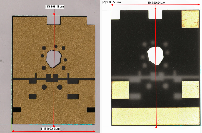
△ Measurement of Sample Accuracy after Processing (Right / Back)
The picosecond pulse width and ultraviolet wavelength “cold processing” characteristics result in a heat-affected zone thickness less than 5 μm , The cutting edge has no heat discoloration, no carbonization blacking, no oxidation yellowing, and the original color and insulation properties of the substrate are completely preserved.For thermally sensitive aluminum nitride materials , this means higher processing quality and yield.
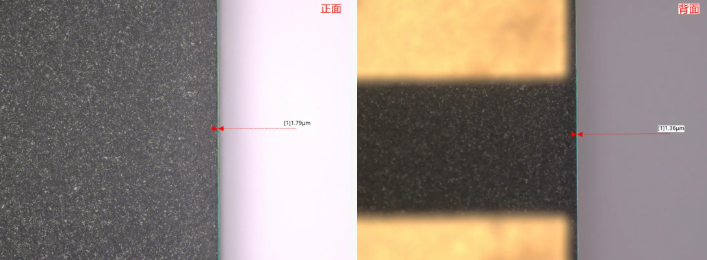
△ Microscopic Effects of Samples after Processing
Edge chipping, microcracks, and burrs are the main bottlenecks affecting ceramic substrate mass production yield. The finished product has a clear and smooth outline and is visible to the naked eye.Microscopic inspection revealed positive chipping at the edge of approximately 1.8 μm , Backside chipping only 1.36 μm . No secondary grinding or trimming is required; it can directly proceed to the soldering, packaging, and assembly processes, reducing post-processing costs and is suitable for high-volume, high-quality production, effectively improving yield.
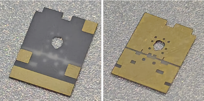
△ Sample Effect after Processing (Right / Back)
Technical preview
In the coming installments of the “Process Notes” series, we will continue to explore the limitless possibilities of laser processing on a variety of different materials, and you are welcome to stay tuned.