
Advanced packaging sits at a materials inflection point. Glass interposers need precision via drilling without taper collapse. Ceramic heatspreaders demand edge quality that mechanical grinding destroys. Organic PCB layers must be machined without delamination. Three materials, three process windows, three separate vendor conversations.
Most answers to “what laser for advanced packaging” come from one of three broken perspectives. Investment analysts frame it as a $40-billion market split across chiplet stacking, hyperscale thermal management, and automotive electrification—but that market view says nothing about which light source solves the actual engineering constraint. Equipment makers (GWEIKE, M-Solv, LPKF) each protect their own process window: the glass vendor emphasizes via diameter control, the ceramic shop touts edge smoothness, the organic integrator pushes HAZ minimization—each selling as if their material is the bottleneck. And suppliers upstream (motion control from PI, optics from Holo/Or, wavelength conversion from others) each optimize for their single component, assuming the laser and everything else will fit around their spec sheet.
Then there’s the light-source perspective. Ultrafast lasers—femtosecond and picosecond systems—aren’t just faster than conventional tools. They work because they deliver energy before heat diffuses into the material bulk. That means cold ablation: removing substrate layers without the thermal shock that cracks glass, chips ceramic edges, or delaminates organic resin bonds. But here’s the counterintuitive part: cold ablation alone isn’t what determines whether you succeed at production scale. What matters is whether your light source can stay cold (tight focus, no beam wander) while pushing the power (average wattage) that production throughput demands. That’s where most approaches break. A 50-watt ultrafast source keeps a beautiful M² (beam quality factor under 1.1) until you try to make it work eight hours a day. A 300-watt source hits production volume fast but thermal lensing creeps the M² from 1.2 to 1.6, and suddenly your process margins collapse across all three materials at once.
We’ve watched this pattern repeat across dozens of packaging lines. One engineering leader put it this way:
“We built the packaging line around what we thought were three separate challenges: drilling glass interposers, shaping ceramic heatspreaders, and cutting organic PCB cavities. Spent 9 months optimizing equipment by equipment. Then we looked at what actually failed: 47 percent loss to either surface cracking on glass, chipped edges on ceramic, or HAZ-induced delamination on organic. The root wasn’t the tooling. Three different materials, three different processes—same root cause: beam quality at full power. Switching to a 200-watt ultrafast source with M² under 1.2 (instead of speccing based on peak power alone) cut scrap to 8 percent. The line didn’t change. The light did.”
That’s the insight that changes how you source. You stop asking “what laser is best for glass?” or “which vendor handles ceramic?” You start asking: is this light-source architecture designed to hold beam quality as power scales? And can it do that across the full 24-hour production cycle, not just for a one-hour qualification run?
Ultrafast lasers enable advanced packaging by using nonlinear absorption (multiphoton ionization) to remove material before thermal damage spreads. Glass, ceramic, and organic substrates all process via cold ablation—no heat-affected zone, no microcracking, no delamination risk. But production yield depends on one constraint that cuts across all three materials: whether your light source can maintain low M² (tight focus, stable beam) while delivering high average power (fast cycle time). A 200–300 watt slab-architecture ultrafast source, typically Nd:YAG or Yb-fiber based at 1030–1064 nanometers, is the industrial standard because it solves the M² versus power tradeoff. Equipment and motion control don’t change the material; light quality does.
Advanced packaging is the fastest-growing segment of semiconductor assembly. Chiplet interconnects demand ±1–2 micrometer precision across substrate stacks with thermal conductivity spanning 1000-fold (silicon to organics). AI accelerators and automotive systems require thermal management that glass and ceramic substrates enable but conventional machining destroys.
The traditional tools (waterjet, plasma, CO₂ laser) each fail in predictable ways. Waterjet leaves delamination cracks from mechanical stress. Plasma leaves residue in deep vias. CO₂ generates 50–100 micrometer heat-affected zones that compromise bondline integrity. Ultrafast processing sidesteps all three by shifting the physics: instead of heating the material, the laser couples energy through nonlinear processes (two-photon or three-photon ionization), ablating material at the focal point while the periphery stays cold.
But “ultrafast” has become a category label, not a specification. A 40-watt fiber laser and a 300-watt slab laser are both ultrafast. The difference between success and scrap at production scale is whether that ultrafast light source can hold precision (low M²) while you’re processing thousands of substrates back to back. That’s the decision every R&D team, sourcing manager, and process engineer faces. And it’s the decision most vendors obscure.
Glass interposers, ceramic heatspreaders, and organic substrates look like three separate process problems. They’re not. Here’s why they’re actually one problem with one solution.
Glass (silica, SiO₂) is transparent to infrared light at 1064 nanometers. A single photon doesn’t couple. But pulse two or three photons at the same location in femtoseconds, and the material ionizes. The ionization happens only at the focal point—the beam waist where intensity is highest. Periphery stays cold. That’s cold ablation.
The engineering variables are taper angle (cone shape of the via), microcracking at boundaries, and stress buildup from repeated drilling. Direct drilling—using GHz repetition rate, shallow pulses, percussion—typically produces 6–8 degree tapers and requires 600 or more passes per via. Costs per good via run $0.12–0.18 after accounting for rework. Modify-and-etch—laser inscribes a line in the glass, then potassium hydroxide or hydrofluoric acid widens it—produces near-vertical walls (2–3 degree tapers) and better yield after copper electroplating, bringing cost-per-good-via down to $0.08–0.11.
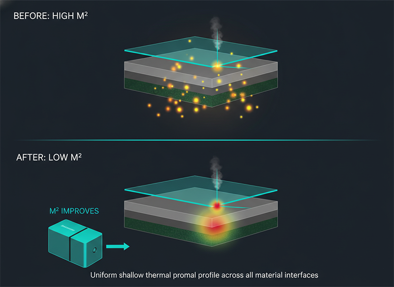
Both routes require the same light-source architecture property: low M². Why? Because you’re drilling 100–200 micrometers deep. The laser beam diffracts and scatters inside the glass. If M² is high (say, 1.8), the beam wanders as it descends, and the bottom of the via loses focus—you get a wide taper and stress concentration. If M² is tight (1.2 or lower), the diffraction is minimal, focus stays centered, and the via profile stays stable. That precision is what keeps stress under control and good-via yield high.
A fiber laser maxes out around 50 watts while holding M² under 1.1. A slab-architecture laser hits 200–300 watts while holding M² under 1.4. In production, that means the slab laser processes the same substrate in one-third the time without losing precision. That’s not a marginal win—it’s 2.5–3 times throughput at the same cost-per-wafer.
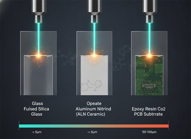
Aluminum nitride and beryllium oxide have thermal conductivity 200–300 times higher than silicon. That’s why they sit between the die and the solder ball in high-power packages. But they’re mechanically fragile. A waterjet or grinding chip propagates into a crack. A CO₂ laser melts the surface.
Ultrafast processing couples nonlinearly into ceramic via two-photon absorption (unlike glass, which is three-photon dominated). The ablation plume is cool, and peripheral heating is minimal. But here’s the constraint that’s identical to glass: if your M² drifts during a production run, the process window collapses. Beveled edge chamfers (15–30 degrees) for solder-fillet strength require consistent edge quality. Precision pockets for thermal-interface attachment require ±0.05 millimeter repeatability. A single chipped edge rejects a $40–80 substrate and costs $200–300 in BGA assembly rework.
The light-source constraint isn’t ceramic-specific. It’s the same M² stability that matters for glass. High-power slab sources (200–300 watts) maintain that M² consistency across an 8–12 hour production shift. Fiber sources plateau earlier and require frequent re-characterization. That’s why ceramic fabs prefer slab architecture.
Epoxy resin (FR-4, ABF, BT) delaminates at glass-transition temperature around 150–180 degrees Celsius. A conventional nanosecond YAG laser thermal couples into the substrate and lifts that temperature. Resin near the hole boundary absorbs heat, expands, and pulls away from adjacent layers. Result: micro-delamination that shows up three thermal cycles later as an open circuit.
Ultrafast ablation removes material before heat reaches the interface. The heat-affected zone stays under 5 micrometers—versus 10–20 micrometers for nanosecond systems and 50–100 micrometers for CO₂. That HAZ depth directly correlates with delamination rate. A via drilled with 4-micrometer HAZ survives 1000 thermal cycles; 20-micrometer HAZ sees 40–60 percent failure by cycle 500.
But here’s what makes this part of the integration problem: glass vias and ceramic edges are processed first. By the time you’re drilling organic cavities, thermal soak from previous steps is already heating the substrate stack. If your light source is inefficient (high M², long dwell time per feature), cumulative thermal load exceeds the organic bondline’s tolerance. Suddenly you’re getting delamination on features that passed single-material testing.
A high-power, stable-M² light source (slab architecture, 200–300 watts) compresses cycle time on each material, keeping total thermal soak under the bondline limit. It’s not a ceramic-specific problem or an organic-specific problem. It’s a system-level constraint that only shows up when you integrate.
Here’s what competitive positioning obscures. A glass-specialist vendor optimizes for via diameter and taper. A ceramic shop optimizes for edge smoothness. An organic integrator optimizes for minimum HAZ. Each publishes specs that make sense in isolation. But stack them on a single substrate, and the real constraint emerges: thermal profile management across the full sequence.
A research engineer working on multi-layer substrate qualification described it this way:
“Through-glass vias were my first 18 months. I tested six routes—direct ablation, modify-etch, percussion, helical. Each with different thermal profiles. Then we integrated glass onto the ceramic substrate test article, and the ceramic delaminated. Not because the ceramic laser interaction was wrong. Because the glass process’s thermal byproduct was heating the interface. We separated the optics, rebuilt isolation. Cost $240,000 in downtime. Then we qualified two organic cavities into the same panel. Different material, same heat-signature problem. The physics that matters isn’t glass-specific or ceramic-specific. It’s thermal-byproduct and soak time. A low-M² source at full power meant we could compress the thermal-duty cycle and cut standoff distance without re-qualifying the entire integration. That’s not an optimization. That’s a rework avoidance.”
That’s the sourcing constraint: not “what laser is best for each material” but “what light-source architecture keeps thermal load uniform across the sequence?”
Most packaging integrators source through different vendors. Glass interposer suppliers (Light Conversion, Fluence) have laser-based drilling lines. Ceramic OEMs (Rogers, Kyocera) have their own laser shops or partner with specialized vendors. Organic-PCB integrators (Meiko, Ibiden) use in-house ultrafast lines or contract with process specialists.
The implicit assumption: each vendor handles their material optimally, and you assembly the board by connecting independent subsystems. That’s the model Light Conversion, GWEIKE, M-Solv, and equipment integrators all sell.
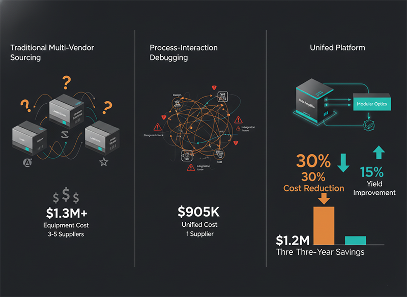
But when you’re sourcing at scale—defining the three-year supply strategy for a chiplet packaging line—you’re managing three single-points-of-failure. Each vendor’s uptime, M&O cost, supply continuity, and process reliability are independent risks. You negotiate three contracts, train three teams, maintain spare parts for three systems, and debug interactions when they occur.
Alternatively: specify a unified light-source platform (standard 1030–1064 nanometer wavelength, supporting all three material processes via software-switched optics and beam-shaping modules). One supplier relationship. One thermal management strategy. One M² monitoring system across the full integration sequence. That’s where sourcing complexity flips from a liability into a strength.
Packaging cost is not cost-per-hour of machine time. It’s cost-per-good-part after accounting for rework, scrap, re-qualification, and supply-continuity risk.
Via diameter: 50 micrometers Via depth: 100 micrometers Array density: 16,000 vias per 200-millimeter wafer Direct-ablation route: 20 milliseconds per via, 600 milliseconds per wafer, plus 12 minutes post-processing (rework inspection) Cost-per-good-via: $0.12–0.18
Modify-and-etch route: 10 milliseconds laser write, 8 minutes chemical etch, 2 percent scrap from etch-mask defects Cost-per-good-via: $0.08–0.11
The chemistry adds cost, but yield is higher because you’re not fighting the two-photon stress mechanism that direct ablation inherits.
Traditional grinding: $18–24 per substrate, plus $200 rework cost on every chipped edge (8–12 percent rejection rate) Ultrafast laser: $8–12 per substrate, <1 percent rejection rate
Annual volume: 50,000 substrates Grinding cost: $1.2 million + $100K rework = $1.3M Ultrafast laser: $500K capital (amortized), $400K operating, $5K rework = $905K Three-year savings: $1.2M
Conventional CO₂ or mechanical drilling: 15–20 percent HAZ-induced delamination rate Ultrafast drilling: <2 percent delamination rate
Volume: 100,000 substrates per year Rework cost per failure: $80–120 (re-drill, re-inspect, re-qualify layer stack) Annual scrap prevention: 15 percent × 100K × $100 = $1.5M
The ROI analysis isn’t about cycle time. It’s about scrap avoidance and supply-chain resilience.
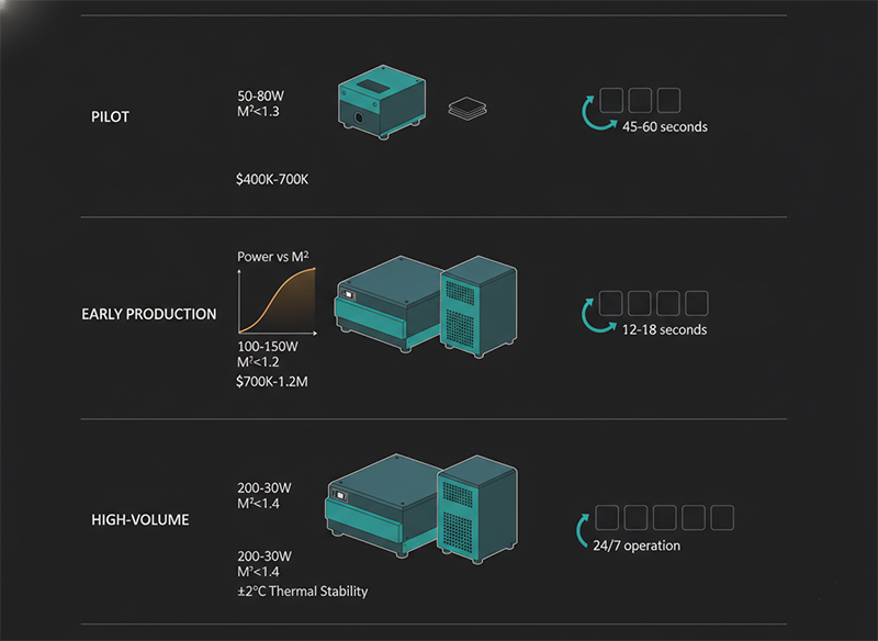
Prototype and pilot production (sub-500 wafers per month): You’re still trading routes and materials. Precision consistency matters more than peak power. Minimum spec: 50–80 watts, M² stable under 1.3, galvanometer beam steering with F-theta optics, and real-time beam-quality monitoring. Cost: $400K–700K. At this scale, accept that you’ll re-qualify processes as volumes scale; that’s normal. Trade speed for learning.
Early production (500–2000 wafers per month): You’ve locked the material choices and process routes. Now throughput becomes cost-critical. You need 100–150 watts, M² under 1.2 sustained across 12-hour shifts, and thermal stability that doesn’t drift process windows. Upgrade to integrated chiller and active beam stabilization if thermal load is >80 watts average. Cost: $700K–1.2M. This is where most vendors stop pitching. They’ll sell you the system and tell you that higher power doesn’t help because “you don’t need it.” Wrong. You’re about to scale.
High-volume production (>2000 wafers per month): You need 200–300 watts slab-architecture source, M² under 1.4 sustained across 24/7 multi-shift operation, and thermal-load management systems that keep substrate temperature within ±2 degrees Celsius across the integration sequence. This isn’t overkill. A single M² drift of 0.2 units cascades to 3–5 percent yield loss at tight tolerances. You need redundancy built in. Cost: $1.2M–2M capital, but per-wafer processing cost ($22–28) amortizes the investment while you’re running production. This is where you flip from cost-center mindset to asset-class ROI.
The counterintuitive move at every stage: don’t specify the highest power you think you might need. Specify the lowest power that holds beam quality under load. A 100-watt source with M² stable at 1.1 often outpaces a 200-watt source with M² creeping from 1.3 to 1.6 by 30–40 percent because the tight-beam process can run narrower feature pitches and fewer re-optimizations per run. Cost-per-good-part is better. Yield is higher. Sourcing is simpler.
There’s a sourcing trap that catches most teams. Advanced packaging lines rarely deploy a single laser vendor across all three materials. It’s understandable: you’re de-risking. Glass vias go to the specialist (Light Conversion, Fluence). Ceramic edges to another shop. Organic cavities to a third. Each vendor has published data. Each looks competent in their domain.
But that sourcing fragmentation creates a hidden cost: process-interaction debugging, supply-chain coordination, and thermal-load management that you’ll own, not the vendors. When a thermal spike from the glass process starts causing ceramic delamination, you’re in the middle. No vendor takes responsibility. You hire a consultant. Downtime extends. Cost compounds.
The sourcing pivot: instead of asking “which vendor is best for glass?”, ask “is this light-source architecture designed to hold M² and thermal stability as power scales?” If yes, you can run all three processes on one platform, manage supply through one relationship, and debug process interactions on unified data. That’s not vendor lock-in. That’s risk reduction.
If you’re sourcing at scale, talking to a supplier directly surfaces details no RFQ will tell you. Real uptime metrics from peer installations running 24/7. M² behavior under thermal load that lab specs don’t capture. Supply continuity during allocation crises. And whether their engineering team has actually debugged the integration problem you’re facing—not just optimized one material in isolation.
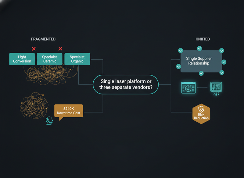
Advanced packaging stacks glass, ceramic, and organic substrates into integrated systems where one material’s process byproduct becomes the next material’s constraint. That’s not a problem you solve with three independent specialists. It’s a system-level challenge that only a light-source perspective reveals: quality at scale depends on whether your ultrafast laser can hold beam quality (low M²) while delivering the power (average wattage) that throughput demands.
That’s why we built slab-architecture sources that reach 200–300 watts while keeping M² under 1.4. Not for the peak power. For the stability. The margin. The ability to run process windows tight enough to make hard-brittle materials work reliably. In advanced packaging, that light-source architecture is the asset. The equipment and motion control are just the means to use it.
Q: Why can’t a compact fiber laser (50 watts, M² under 1.1) deliver the same results as a 200-watt slab laser?
A: Fiber lasers achieve excellent beam quality by sacrificing average power and duty cycle. At 50 watts, processing one wafer takes 45–60 seconds because thermal buildup limits how long the laser can run continuously. A 200-watt slab laser processes the same wafer in 12–18 seconds while holding M² under 1.4, delivering 2.5–3 times throughput. In production cost-per-good-part, high-power-with-acceptable-M² beats peak-beam-quality-at-low-power every time.
Q: What’s the typical heat-affected zone (HAZ) depth for ultrafast versus conventional lasers on organic PCB?
A: Ultrafast (femtosecond/picosecond) achieves HAZ under 5 micrometers. Nanosecond YAG: 10–20 micrometers. CO₂: 50–100 micrometers. Each doubling of HAZ depth roughly doubles the delamination risk after thermal cycling, so the step from ultrafast to conventional costs you 10–15 percent yield on high-reliability applications.
Q: Can I retrofit an existing packaging line with an ultrafast laser, or is it a full rebuild?
A: Depends on your motion hardware. If galvanometer-based, retrofitting is often feasible (swap laser head, re-characterize beam path, update control software). If you’re running legacy mechanical X-Y stages, you’re looking at a platform rebuild to accommodate the precision and thermal management an ultrafast system requires.
Q: How much does ceramic heatspreader edge quality actually impact final yield?
A: Edge defects (micro-cracks, chipping) are responsible for 40–60 percent of late-stage BGA assembly rejects in packages over 200 pins. In high-volume manufacturing (millions of units per year), optimizing ceramic edge-prep process and tooling pays back in weeks. A $5K process refinement avoids $200–300 per-unit rework cost at scale.
Q: Does laser pulse width matter if beam quality (M²) is already low?
A: Yes, but indirectly. M² controls spot size and focus depth. Pulse width controls the ablation mechanism (multiphoton vs. thermionic coupling). Shorter pulses (femtosecond, sub-100 femtoseconds) enable pure nonlinear coupling with minimal heat. Picosecond pulses (10–100 picoseconds) balance speed and precision. Ultra-wide pulses (nanosecond, >500 picoseconds) couple thermally—even with low M², you inherit heat-affected zone and edge damage. For advanced packaging, picosecond to short-femtosecond is the sweet spot.
Q: What wavelength should I specify for multi-material integration (glass + ceramic + organic)?
A: 1030–1064 nanometers (Nd:YAG or Yb-fiber-amplified systems) are the industrial standard for all three materials. Both wavelengths couple via nonlinear absorption across glass, ceramic, and organic substrates. Longer wavelengths (1550 nanometers Er:glass) or shorter (355 nanometers UV) lock you into single-material processes. Avoid mid-run wavelength switching unless your process engineering team has significant ultrafast integration experience.
Q: Why do some suppliers claim 50-micrometer via holes with commercial equipment while others struggle at 75 micrometers?
A: Claimed specs assume ideal lab conditions (pristine material lots, new tooling, short runs, careful fixturing). Real production scales with material lot variation (glass residual stress, ceramic density scatter), 24/7 thermal drift (M² creep, thermal lensing), and statistical yield targets (>95 percent good vias is safe; <85 percent triggers rework cost spiral). Suppliers reliably hitting 50 micrometers are running sub-0.9 M² sources or using high-overscan redundancy (high cost-per-part). Ask for production data, not lab specs.
Q: How do I know if my current laser line’s M² is stable across a production shift?
A: Install a beam-profiler diagnostic every 2–4 hours during full-load operation (not during idle time). Measure beam waist size, divergence angle, and calculate M². Plot drift over the shift. If M² climbs more than 0.1–0.15 units, you have thermal lensing (usually thermal load on the amplifier) or alignment creep (mechanical stability issue). Both are fixable: better thermal management or stiffer optical mounting. Don’t ignore it—creep is invisible in per-part inspection but shows up as yield loss after 200–500 parts.