
The cleaner pulse can be the one that cracks your vias. That sentence sounds wrong, which is exactly why so many TGV processes get specified backward — chosen on entrance-hole photos and drilling-speed charts, then quietly failing at metallization. We have watched a femtosecond recipe win on paper and lose on the wafer.
“We specified femtosecond for the TGV line — shortest pulse, smallest taper, the defensible call for a 200 µm Borofloat interposer. On paper it won: taper near 6°. Then inspection came back. The femtosecond holes carried microcracks and backside ablation from the high peak intensity — the ‘cleaner’ pulse was seeding the defect that kills vias after metallization. We moved to 5 ps at 25 µJ over 600 passes. Taper rose to about 7.3°, but the array survived thermal shock to 950 °C with residual stress under 9 MPa. The variable we treated as the quality guarantee was the wrong one to optimize.” — process engineer, glass interposer TGV qualification
This matters because ultrafast laser TGV drilling has reached the point where the physics is no longer the differentiator. Every credible supplier can make a hole in glass. What separates a production process from a demonstration is which route you choose and which number you optimize.
Ultrafast lasers drill through-glass vias by nonlinear, multiphoton absorption. Glass is transparent to the beam at low intensity, so energy only couples in where the focused pulse is intense enough to trigger multiphoton and avalanche ionization. Because the pulse ends before heat spreads — “cold” ablation — you get high-aspect-ratio holes with a small heat-affected zone. Two production routes exist: direct laser ablation, and laser modification followed by chemical etching.
People search this question at a specific moment: they are about to commit capital and a process flow to glass-core packaging, and the stakes have climbed. Glass interposers now sit under AI accelerators, high-bandwidth memory, and co-packaged optics, where via reliability and density feed directly into signal integrity and yield.
In our work qualifying TGV processes, the recurring failure is not an inability to drill glass. It is a mismatch between the metric a team optimized and the metric their product actually needed. A line gets specified around taper, or around vias per second, and then loses wafers to cracks that only appear two process steps later.
So this article does not stop at the mechanism. It covers how the two laser routes differ, why “cost per good via” beats drilling speed, why packaging density is a stress problem rather than a spot-size problem, and how to read a supplier’s data so an as-drilled photo never decides a production buy. Each section is built around a decision you are likely making right now.
A through-glass via is a high-aspect-ratio hole, later filled with metal to carry signals vertically through a glass substrate. Forming it cleanly is hard because glass is brittle, and any drilling method can seed chips or microcracks that compromise the wafer.
The ultrashort pulse gets around glass’s transparency through nonlinear absorption. At the focus, peak intensity is high enough that the material absorbs through multiphoton ionization, builds a free-electron plasma, and ablates — all before the lattice has time to heat. That timescale is why thermal damage stays limited and why feature control is so tight.
Pulse duration sets the trade. Shorter pulses raise peak intensity and can cut taper, but in direct drilling that same intensity can drive backside ablation and microcracking. As the Opening Hook scenario showed, a picosecond pulse often produces the crack-free result a femtosecond pulse does not. Reported work using a 1030 nm source above 200 µJ has also reached aspect ratios near 1:24 at sub-50 µm diameters, with 250 fs pulses drilling roughly 1.7× deeper than picosecond pulses — useful range, but range that still has to be matched to your failure mode.
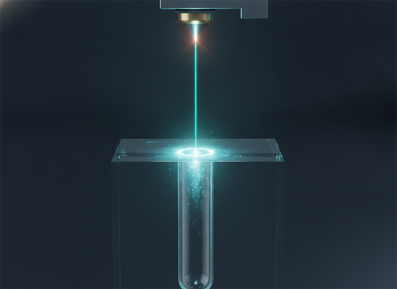
Direct ablation removes material pass by pass with a beam steered by a galvo scanner through an F-theta lens. In GHz burst mode, each pulse is split into sub-pulses a few hundred picoseconds apart; heat and plasma pressure accumulate in the channel and expel molten material upward, which makes the process both faster and cleaner than single-pulse drilling.
The appeal is throughput and simplicity. A 1 mm-deep via can form in tens of milliseconds, putting several million vias on a wafer in under an hour, with no wet chemistry in the flow. Near-taperless holes are achievable with tuned burst parameters.
The limits show up with depth and geometry. Deep channels drilled with short focal lengths can curve once they propagate past a point, and the geometry you can dial in is narrower than the etch route offers. Quality is also sensitive to burst settings, so the process window needs real characterization, not a single golden recipe.
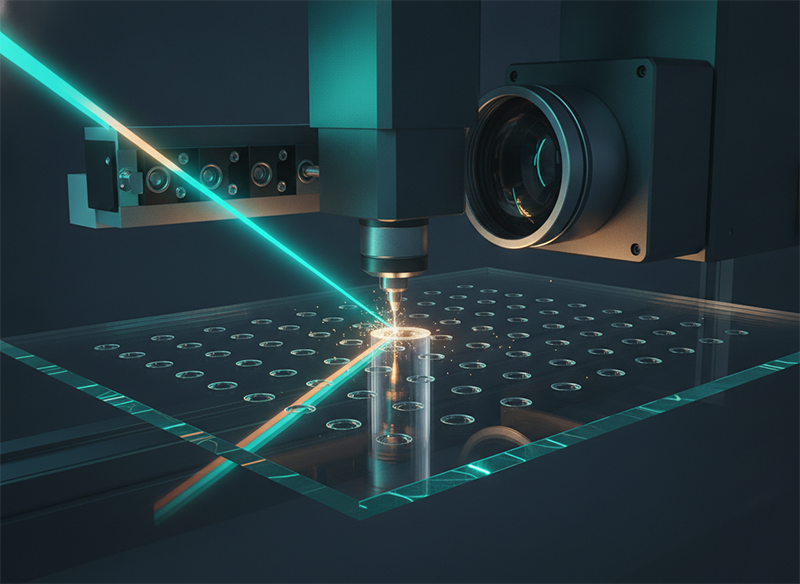
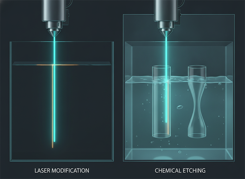
The second route writes a modification, then etches. A Bessel beam creates a continuous, narrow modified zone through the full glass thickness in essentially one shot. The part then goes into KOH or HF, where modified glass etches far faster than the surrounding material.
This is the route to reach for when geometry is the requirement. Etch temperature and concentration set the profile, so straight walls, steep sidewalls, or hourglass shapes all come from the same modification step, and a single modified line can open into diameters from roughly 10 µm to over 100 µm. Sidewall quality for plating is excellent.
The cost is time and chemistry. The etch step runs for hours, throughput depends on how many holes were modified first, and HF/KOH handling adds safety and sustainability overhead. Initial material cost is higher because the etchant works on the whole substrate, not only the via.
Here is the comparison in one view:
| Priority | Direct ablation | Modify + etch |
|---|---|---|
| Raw throughput per via | Strong | Weaker (hours of etch) |
| Tailored geometry (hourglass/steep) | Limited | Strong |
| Sidewall quality for plating | Good | Best |
| Deep / stacked glass | Long-focal works | Strong |
| CapEx and footprint | Lower | Higher (etch line, chemistry) |
| Wet-chemistry handling | None | HF/KOH |
If you are still weighing routes at this stage, the next two sections are where most evaluations go wrong.
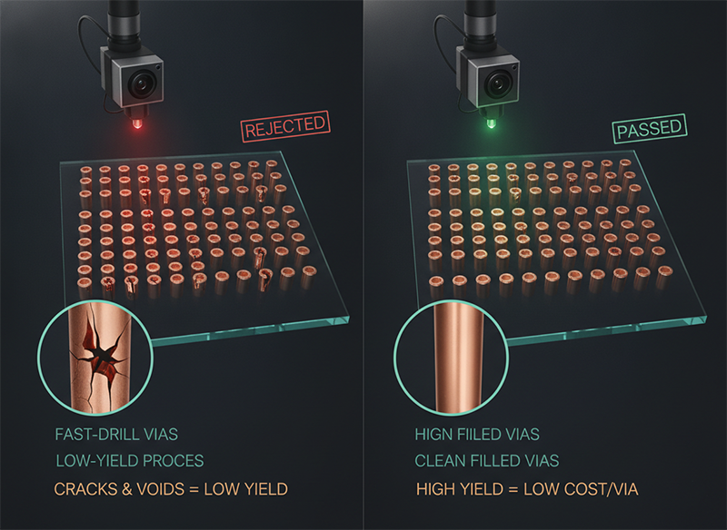
Direct ablation drilling a via in about 20 ms is a compelling pitch. On pure throughput it wins. But drilling speed is not the number that decides production economics — cost per good via after metallization is.
“The pitch was simple: ablation drills a via in 20 ms, millions per wafer in under an hour — why run a multi-hour etch? So we benchmarked it honestly. On pure throughput, ablation wins. But the metric that mattered was cost per good via after metallization. Ablation’s residual stress and taper variation cost us copper-fill voids and cracks at CMP — scrap that never shows on a drilling-rate chart. For our void-free, straight-wall spec, laser modification plus controlled etch came out lower on cost-per-good-via despite being slower. The fast process was only fast until we counted the wafers we threw away.” — R&D lead, TGV process-route selection
When you benchmark suppliers, ask for cost per good via after the downstream steps your part actually runs — not vias per second on bare glass. A number measured before metallization tells you almost nothing about your final cost.
It is natural to treat interconnect density as an optics problem: tighter focus, tighter pitch. The glass has the deciding vote.
“We assumed density was a beam-spot problem, so we pushed via pitch down to 160 µm on a 125 µm-via array. The spot handled it; the glass didn’t. Polarimetry showed residual stress in the ~35 µm wall between vias spiking to 31 MPa, and cracks appeared between the holes, not in them. Back off to 180 µm pitch and stress dropped to about 20 MPa, crack-free. What set our maximum density wasn’t the laser’s resolution — it was accumulated thermal stress in the wall staying under the glass’s crack threshold.” — process integrator, high-density glass interposer TGV array
This is also where average power and heat management earn their keep. More power raises throughput, but only a process that controls heat accumulation lets you use it without stacking the residual stress that caps density. Source architecture matters here — high-power slab integrated amplification in the 100–300 W range exists to deliver usable power without adding the stress that cracks the wall between vias.
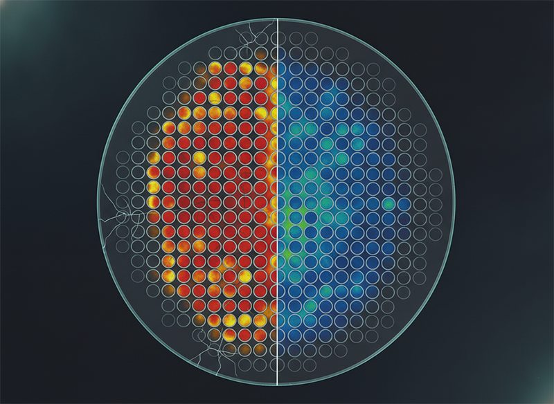
Use this to narrow the route quickly. If your part needs tailored geometry — hourglass profiles, steep straight walls, tight critical-dimension control for plating — choose laser modification plus etch, and accept the cycle time. If you need very high via counts, a simple flow, and no wet chemistry, choose direct ablation and budget for process-window characterization. If you are drilling thick or stacked glass, favor long-focal ablation or the etch route. And whichever you pick, set your acceptance metric as cost per good via after metallization, and set your maximum pitch by residual stress, not spot size. When two routes look close, the deciding factor is almost always your glass type and your downstream fill spec — not the laser’s headline number.
Two variables decide more than the laser itself. First, the glass: Borofloat, fused silica, Eagle XG, and AF32 absorb, conduct heat, and crack differently, so a recipe proven on one does not transfer — ask for validation on your substrate. Second, the evidence: request residual stress maps and post-thermal-cycle crack data, not as-drilled SEM. If you are sourcing at scale, talking to a supplier directly can surface details no product listing will tell you — the process window, the failure modes, the numbers measured after metallization.
The femtosecond line that cracked taught the same lesson every TGV evaluation eventually teaches: the number that photographs best is rarely the number that ships. Taper, drilling speed, and spot size are easy to measure and easy to over-trust. Cost per good via, residual stress, and behavior after metallization are harder to measure and decide everything. Pick the route for your geometry and your glass, prove it on your substrate, and judge it on the wafers that survive — not the holes that look good on day one.
What pulse duration is best for TGV drilling?
There is no universal answer. In direct drilling of borosilicate glass, femtosecond pulses give the smallest taper but can introduce microcracks and backside ablation, while a roughly 5 ps pulse often produces crack-free vias at slightly larger taper. Choose against your dominant failure mode rather than assuming shorter is better.
Direct ablation or laser modification plus etch — which is better?
Ablation is faster per via and uses no wet chemistry; modification plus etch gives better geometry control and sidewall quality but takes hours and needs HF or KOH. The right choice depends on via count, geometry, glass type, and cost per good via — not on drilling speed alone.
How fast is ultrafast laser TGV drilling?
Direct ablation can form a 1 mm-deep via in tens of milliseconds, placing several million vias on a wafer in under an hour. Large-diameter drilling is much slower and may not meet electronics-industry throughput, which is part of why panel-level scaling and etch parallelism exist.
Why do my vias crack only after metallization?
Residual stress and microcracks seeded during drilling grow under the thermal and mechanical load of metallization and thermal cycling. As-drilled inspection can look clean while the via is already compromised, which is why stress and post-cycle data matter more than entrance photos.
What limits how densely I can pack TGVs?
Usually accumulated thermal stress in the wall between vias, not the laser spot size. Below a certain pitch the wall cracks; in one array, 160 µm pitch reached 31 MPa with cracks while 180 µm dropped to about 20 MPa, crack-free.
Does higher average power increase throughput?
It can, but only with heat-accumulation control. More power without that control raises residual stress and lowers yield, so usable throughput depends on both the source and the processing strategy.
Which glasses can ultrafast lasers drill for TGVs?
Common substrates include Borofloat 33, fused silica, Eagle XG, and AF32. Each behaves differently under the same parameters, so a process validated on one glass should be re-qualified on yours before production.
How do I judge TGV quality from a supplier?
Ask for cost per good via after metallization, residual stress maps, post-thermal-cycle reliability, and achievable taper, aspect ratio, and pitch at your target yield — measured on your substrate, not a reference glass.


What Laser Source Specs Matter Most for Through-Glass Via (TGV) Processing? - Laserion Photonics Technology Co., Ltd says:
[…] with GHz-class burst packets—removes glass in a single tool path without a wet bench. Selective laser etching (modification then HF or KOH etch) trades a chemical step for crack-free channels, steep walls, and […]