Most laser processes are judged by how cleanly they remove material. Laser lift-off is judged by the opposite — how well the material you are not trying to touch survives. That inversion is the whole reason LLO is its own discipline, and it is the first thing that trips up engineers who arrive from cutting or drilling.
“Every laser process I’d run before was about removing material cleanly. Laser lift-off flipped that. The material the laser interacts with — the interface layer — is sacrificial; the thing that has to come out perfect is the device layer we’re trying not to touch. We kept optimizing the ablation and wondering why yield lagged, until it clicked that the metric wasn’t a clean cut, it was an undamaged film released intact. In LLO, the product is what survives the laser, not what the laser removes.” — process engineer, LED device manufacturing
I take that account seriously because it reframes the entire process. In laser lift-off, success is measured on the device layer you release, not on the interface you decompose. This article explains what LLO is, how the process works, and the requirements — wavelength, energy window, and beam uniformity — that decide whether the layer comes off intact.
Laser lift-off (LLO) is a process that uses a laser to separate a thin device layer from its carrier substrate without mechanical contact. The laser passes through a transparent carrier — such as sapphire or glass — and is absorbed at the interface, where it decomposes a thin sacrificial region and releases the device layer above it. The process depends on three requirements: a wavelength the carrier transmits but the interface absorbs, an energy density inside a narrow window, and a uniform beam across the whole field.
Laser lift-off sits at high-value points in manufacturing. It separates GaN LED and micro-LED layers from sapphire so they can be transferred to better carriers, and it releases flexible display films — polyimide on a glass carrier — to make bendable screens. In both cases, the layer being lifted off has already had enormous value added to it. Damage it during release and you scrap a finished device, not a blank.
That is what makes LLO unforgiving. The laser has to deliver enough energy to release the layer but not so much that it harms the device it is freeing — and it has to do that uniformly across a full panel. Unlike cutting, where a more aggressive setting often means a cleaner result, LLO punishes both too little and too much.
Across LLO work, the engineers who hold yield treat it as a release problem governed by selective absorption and uniformity, not a removal problem governed by power. The sections below explain how the process works and walk through each requirement that decides whether the device survives.
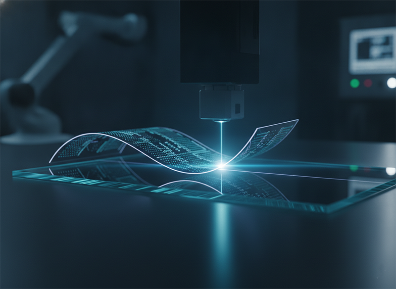
Laser lift-off separates a functional thin film from the substrate it was grown or coated on, without touching it mechanically. The classic case is a GaN LED on sapphire. Intense ultraviolet light is sent through the sapphire, which is transparent to it, and absorbed strongly at the GaN layer at the interface. The absorbed energy chemically decomposes the GaN near that interface — releasing gallium droplets and nitrogen — which detaches the GaN film from the sapphire so it can be transferred to a carrier with better thermal or optical properties.
The same principle drives flexible-display manufacturing. A polyimide film is coated on a glass carrier, the laser passes through the glass, and the energy releases the polyimide so the flexible device can be lifted off intact. In every variant, the pattern is identical: the laser reaches through a transparent carrier and acts only at the interface, leaving the device layer above it free and undamaged. The interface is sacrificial; the device is the product.

The most common mistake is treating LLO as a power problem.
“We approached LLO like a power problem — find the energy that releases the layer, turn it up until it lets go. It half-worked and damaged the device. The fix wasn’t tuning power; it was wavelength. The carrier has to be transparent to the beam while the interface absorbs it — get that wrong and you’re either heating the wrong layer or cooking the device through it. Once the wavelength was matched to pass through the carrier and stop at the interface, the energy window opened up. LLO isn’t about how much energy — it’s about putting it exactly where the carrier ends and the device begins.” — process engineer, flexible display manufacturing
LLO works on selective absorption: the carrier must transmit the wavelength while the interface absorbs it. That is why GaN LLO uses ultraviolet light — sapphire is transparent to UV, and GaN absorbs it strongly, so the energy deposits exactly at the interface and nowhere else. Choose a wavelength the carrier absorbs, and you heat the wrong layer or drive energy through into the device. Wavelength is not a tuning parameter in LLO; it is the foundation that makes the process possible. Get it right, and the energy lands where the carrier ends and the device begins.
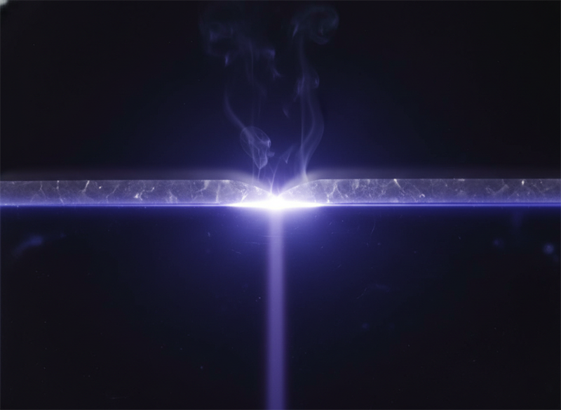
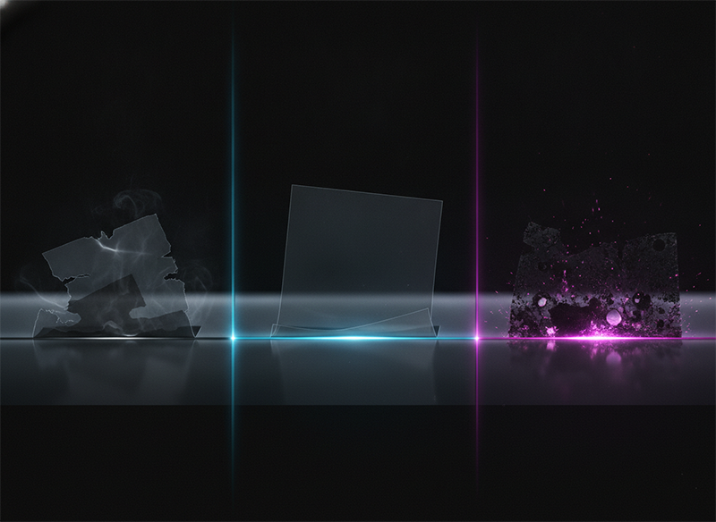
Once the wavelength is right, the energy density has to land inside a narrow window — and the window is bounded on both sides. Too little energy and the interface does not fully decompose, so the layer releases incompletely and the film tears as it comes off. Too much energy and the excess damages the device layer you are trying to protect, through heat or debris.
The numbers make the window concrete. For polyimide on glass, lift-off has an optimum around a specific fluence, while pushing well above it produces carbonization and debris that contaminate the film. This is the opposite of an “aggressive is cleaner” process. In LLO, the right answer is a precisely controlled dose, and reliability comes from holding that dose, not from maximizing it.
Pulse duration adds another lever. Conventional LLO uses nanosecond UV pulses, but ultrashort picosecond and femtosecond pulses limit thermal diffusion, which can reduce the crystal damage induced during release — a meaningful gain where the device layer is sensitive.
A process that works on a test coupon can still fail at scale, and the reason is usually uniformity.
“Our LLO process hit spec on a test coupon — clean release, undamaged film, beautiful. It fell apart on a full panel. The beam’s energy varied across the field, so where it ran hot it damaged the device layer and where it ran cold the film tore on release. The coupon never showed it because it was small enough to sit in the uniform part of the beam. The number that decided panel yield wasn’t peak performance — it was beam uniformity. A flat, even fluence across the whole field beat a higher peak that varied.” — manufacturing engineer, panel-scale device transfer
Because the LLO energy window is narrow and bounded on both sides, any variation across the beam pushes part of the field out of the window. Where the beam runs hot, it crosses into device damage; where it runs cold, it falls short of full release and the film tears. A small coupon hides this by sampling only the uniform center of the beam, so it passes while the full panel fails. This is why a flat-top — top-hat — beam profile is a core LLO requirement: an even fluence across the whole field keeps every point inside the window. At panel scale, uniformity beats peak performance.
| LLO requirement | Why it matters |
|---|---|
| Wavelength (selective absorption) | Carrier must transmit, interface must absorb |
| Energy density (narrow window) | Too low tears the film; too high damages the device |
| Beam uniformity (flat-top) | Keeps every point of a panel inside the energy window |
| Pulse duration | Ultrashort pulses limit thermal damage to the device |
The table is the short version of every LLO qualification: get all four right together, because any one of them out of range fails the device.

If you are setting up laser lift-off, start with wavelength — confirm the carrier transmits it and the interface absorbs it, because no amount of energy tuning fixes the wrong wavelength. Then map the energy window on your actual stack and run inside it, not above it; qualify the upper bound where device damage and debris begin, not just the lower bound where release starts. Demand a flat-top beam and verify uniformity across the full field, not a coupon, since panel yield lives or dies on it.
Choose pulse duration by how sensitive your device layer is: nanosecond UV is the established route, while ultrashort pulses can reduce crystal damage where the device cannot tolerate heat. Judge the whole process on the released layer — its integrity, not the cleanliness of the interface you decomposed. The carrier and the sacrificial region are means; the surviving device is the product.
A few variables decide more than the laser alone: your carrier and device materials and their absorption, your device layer’s sensitivity to heat and debris, your panel size, and the uniformity your tool can hold across it. Each shifts the wavelength, the energy window, and the beam requirements.
Those details are hard to settle from a datasheet. If you are bringing an LLO process toward production, talking to an application engineer who has released your material stack can surface trade-offs no product listing will tell you.
The engineer who kept optimizing the ablation learned that LLO measures success on the layer the laser is supposed to leave alone. That is the quiet truth of laser lift-off: it is not a removal process wearing a different name, but a release process where the product is whatever survives. Match the wavelength to the interface, hold the energy inside its window, keep the beam flat across the panel — and the device comes off intact, which is the only result that counts.
What is laser lift-off (LLO)? Laser lift-off is a non-contact process that uses a laser to separate a thin device layer from its carrier substrate. The laser passes through a transparent carrier and is absorbed at the interface, decomposing a thin sacrificial region to release the device layer above it without mechanical force.
How does laser lift-off work? The laser is sent through a carrier that is transparent to its wavelength and absorbed at the interface to the device layer. The absorbed energy decomposes a thin region at the interface — for GaN on sapphire, breaking GaN into gallium and nitrogen — which detaches the device layer so it can be transferred to another carrier.
What is LLO used for? LLO is used to separate GaN LED and micro-LED layers from sapphire substrates for transfer to better carriers, and to release flexible-display films such as polyimide from glass carriers. In both, it frees a high-value device layer intact so it can be moved to a substrate with better properties.
What wavelength is used for laser lift-off? It depends on the materials. The wavelength must be transmitted by the carrier and absorbed at the interface. GaN-on-sapphire LLO uses ultraviolet light because sapphire is transparent to UV while GaN absorbs it strongly, depositing the energy exactly at the interface.
Why is GaN LED lift-off done through the sapphire? Because sapphire is transparent to the UV wavelength used, the light passes through it and is absorbed at the GaN interface. This lets the energy decompose GaN at the interface and release the LED layer without the beam having to pass through or damage the device layer itself.
What damages the device layer during LLO? Too much energy, a non-uniform beam, or the wrong wavelength. Excess fluence causes heat damage, carbonization, and debris; a non-uniform beam pushes hot spots past the damage threshold; and a poorly matched wavelength drives energy into the device instead of stopping at the interface.
Why does beam uniformity matter in LLO? The LLO energy window is narrow and bounded on both sides, so any variation across the beam pushes part of the field out of it — damaging the device where it runs hot and tearing the film where it runs cold. A flat-top beam keeps every point of a full panel inside the window, which is what holds yield at scale.
Nanosecond vs ultrashort-pulse LLO — what’s the difference? Conventional LLO uses nanosecond UV pulses. Ultrashort picosecond and femtosecond pulses limit thermal diffusion, which can reduce the crystal damage induced in the device layer during release. Ultrashort pulses are attractive where the device is heat-sensitive, at the cost of more complex sources.